Equipment for growth and characterisation
of thin films and nanostructures
(for larger photographs please click)
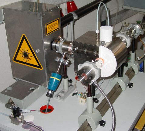
| Pulsed Laser Deposition PLD of thin films using excimer laser LPX 305i and five deposition chambers | 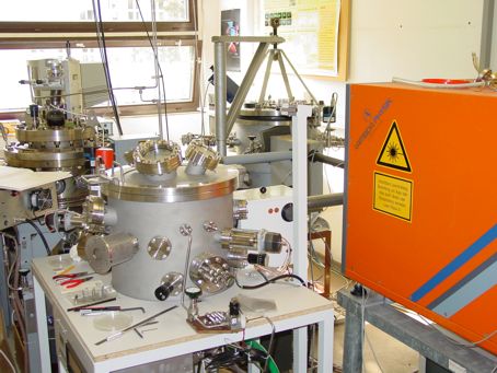 |
| PLD-G-chamber up to 4-inch substrate
diameter, multi-target equipment |
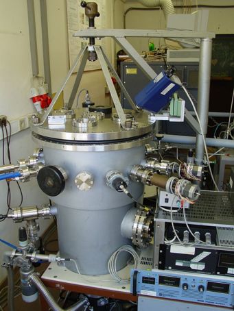 |
| PLD-M-chamber with
heater for 15x15 mm² substrates, multi-target equipment,
RF-radical source |
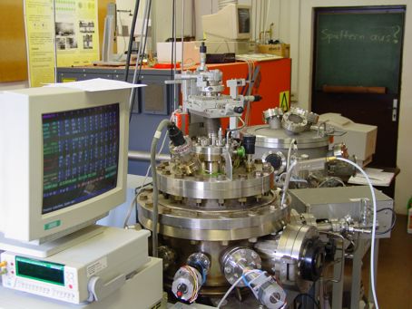 |
| PLD-S-chamber
with 4-inch diam. heater, multi-target equipment |
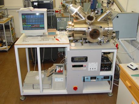 |
| PLD-E-chamber with multi-target equipment, 3-inch diam. heater, in-situ spektroscopic ellipsometry. |  |
| PLD-Q-chamber
for gas pressure in mbar-range, for nano-heterostructures
|
 |
| DC-sputtering chamber for Au, Pt, Ti, Cr, Ag,... |  |
| Surface analysis of structure and morphology by electron diffraction RHEED | 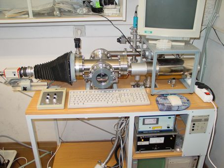 |
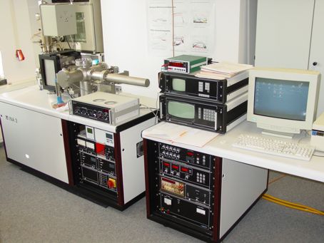
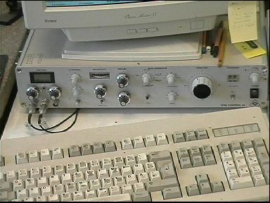
| Secondary
neutrals mass spectrometry SNMS Leybold
INA 3 for chemical analysis and depth profiling
|
 |
| Surface
profiler DEKTAK 3030 |
 |
| Scan of critical current density of
double-sided high-Tc superconducting thin films up to 71 x 75 mm² area |
 |
| RCL-measurement with control of sample temperature from -35 up to +85°C | 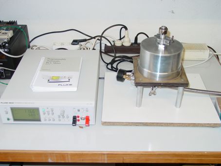 |
| Scanning Tunneling
Microscope STM
"Beetle STM" |
 |
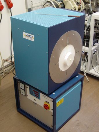
| Sintering
furnace up to
1200°C (chamber) and 1800°C (tube),
ball mills,
press moulds for PLD target preparation, in tube furnace also thermal
growth of ZnO-nanostructures. |
 |
| Microwave vector network analyser Anritsu-Wiltron 37347A up to 20 GHz. |  |
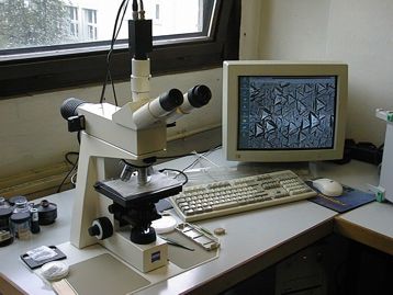
| Zeiss optical
microscope Axiolab with
CCD-camera |
 |
Michael Lorenz, 08 March, 2004