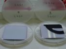
Large-area double-sided YBa2Cu3O7-x
thin films on R-plane sapphire wafers (size 71 x 75 mm²) from PLD
S-chamber, suitable for
microwave
applications.
The reproducible PLD YBCO process is space qualified by
Robert BOSCH GmbH
Stuttgart (Tesat Spacecom Backnang).
|
|
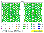
Homogeneous,
side-selective scan of critical current density of large-area PLD
YBCO thin films measured by inductive method
jc-scan Leipzig.
|
|
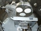
8-inch diam. PLD heater
for simultaneous processing of three 3-inch diam. wafers (supported by
SMWK Dresden).
The substrate
heater principle for optically transparent sapphire wafers
is patent
pending by R. BOSCH
GmbH Stuttgart
(Hochmuth, Lorenz, Natusch, No.
102 55 453.7 of 28.11.2002). |
|
3-channel
input multiplexer demonstrator by BOSCH, Stuttgart, using planar
HTSC YBCO passband channel filters, developed for the BOSCH space
experiment in 2000.
|

|
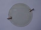
Nominally
undoped 2-inch
diam. ZnO thin films on sapphire deposited in
PLD E-chamber show laterally homogeneous high structural quality.
|
|
Undoped
ZnO
thin films with state of the art electron mobility at 300 K,
deposited in M-chamber by our guest scientist Evgeni Kaidashev, Russia. |

|
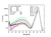
Doped
ZnO
thin films with high luminescence yield around 3.3 eV
at 300 K. The material and process will be patent pending.
|
|
ZnO-MgO
(x 9.5) Bragg resonator mirrors on sapphire deposited in PLD E-chamber.
Visible is the reflection of a
lamp used for illumination.
|

|
ZnO
nanocrystals on sapphire grown by novel high-pressure PLD process in
Q-chamber.
|

|
Our
friend Masa from Japan, who spent one nice year in our group, together
with Dieter, who constructed and built all home-made equipment of
PLD workgroup.
|

|
| From
left: Holger, Evgeni together with his wife Olga, Mrs. Ramm, Michael,
and Dieter celebrating Dieters birthday in our favorite Chinese
restaurant. |

|

