


Address
Staff
Open positions
BSc/MSc thesis topics
Teaching
Research
Publications
Seminar
Press
Internal
Links
Graduate School
BuildMoNa
latest news:
Research Report
HLP 2023
|
Research Methods
|
For execution of our research agenda we employ various
experimental methods and theoretical routines, ranging from thin film deposition, the characterization of structural, electrical and optical properties
to device fabrication and characterization.
Our vision: From deposition to device
|
|
Thin Film Epitaxy and Deposition
In pulsed laser deposition (PLD), a ceramic target is ablated by pulses from a high power laser. From the developing plasma, particles are
deposited onto the heated and rotating substrate.
Using PLD we perform epitaxy of oxide and nitride thin films and heterostructures (quantum wells, superlattices, ...)
in material systems such as (Mg,Zn)O,
(In,Ga,Al)2O3, ZnFe2O3, La(Ni,Mn)O3, BiFeO3, BaTiO3 and TiN.
Using sputter methods (Kathodenzerstäubung) we deposit amorphous semiconductor thin films and thin films of copper iodide.
Also we use reactive sputtering for the creation of Schottky contacts on various oxide semiconductors.
With plasma-enhanced chemical vapor deposition (PECVD) we deposit insulators and dielectric layers
in the Si/SiOxNy system.
Using thermal evaporation we deposit metals (Au, Al, Ti, ...) for Ohmic and Schottky contacts. Also oxide
nanostructures are fabricated using carbo-thermal evaporation schemes.
More on pulsed laser deposition
|
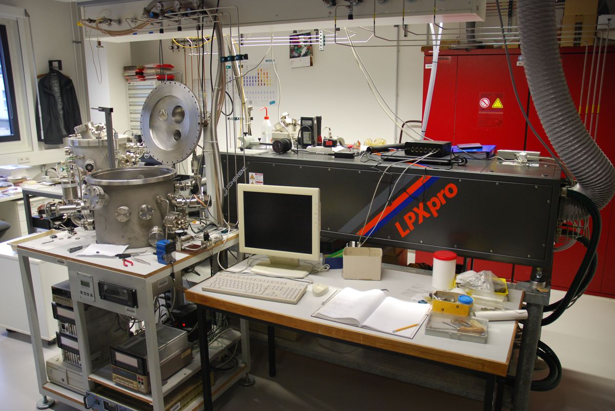
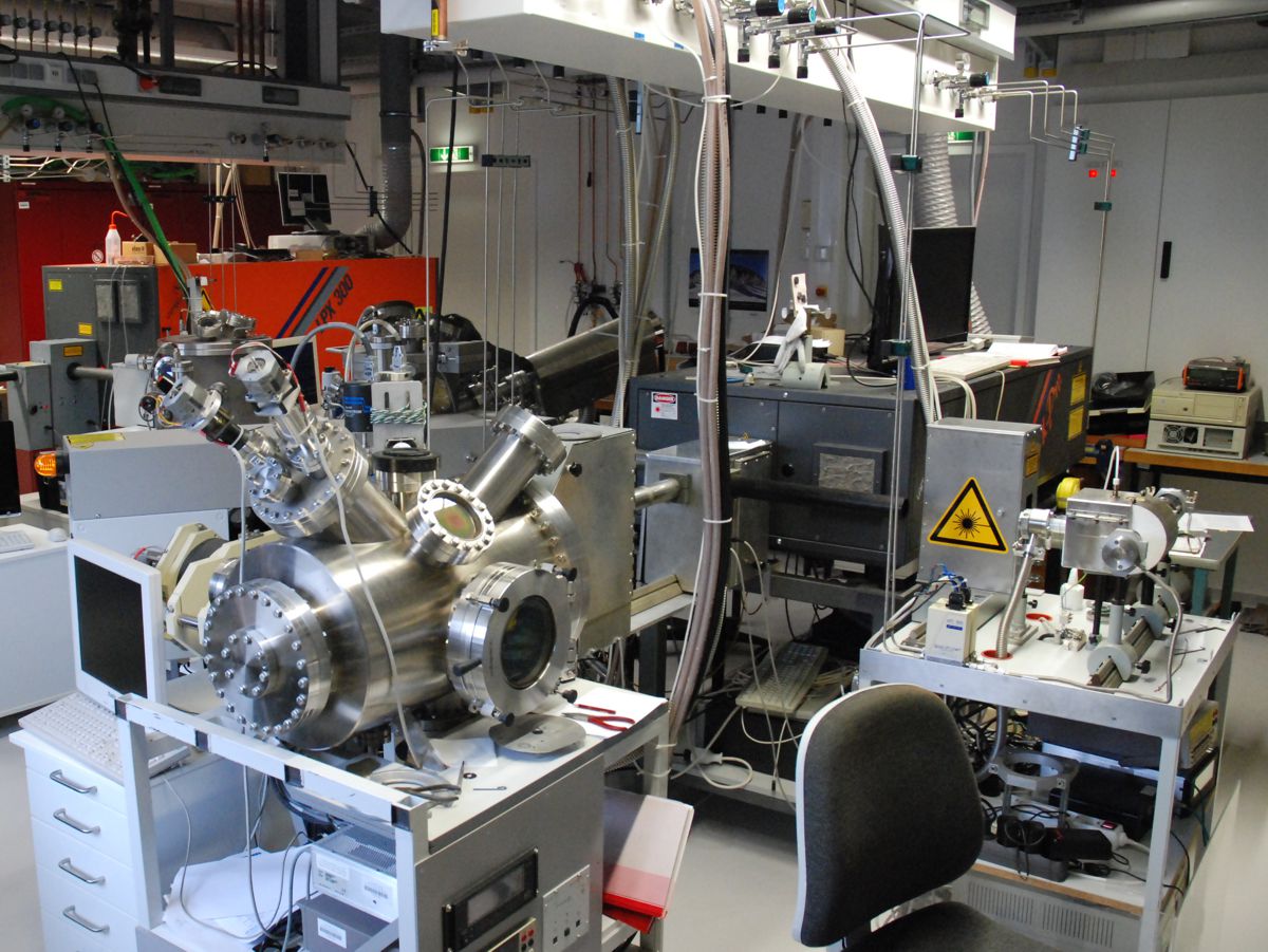
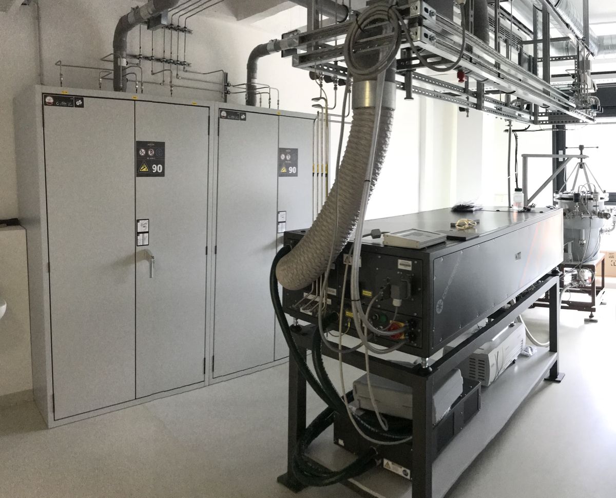
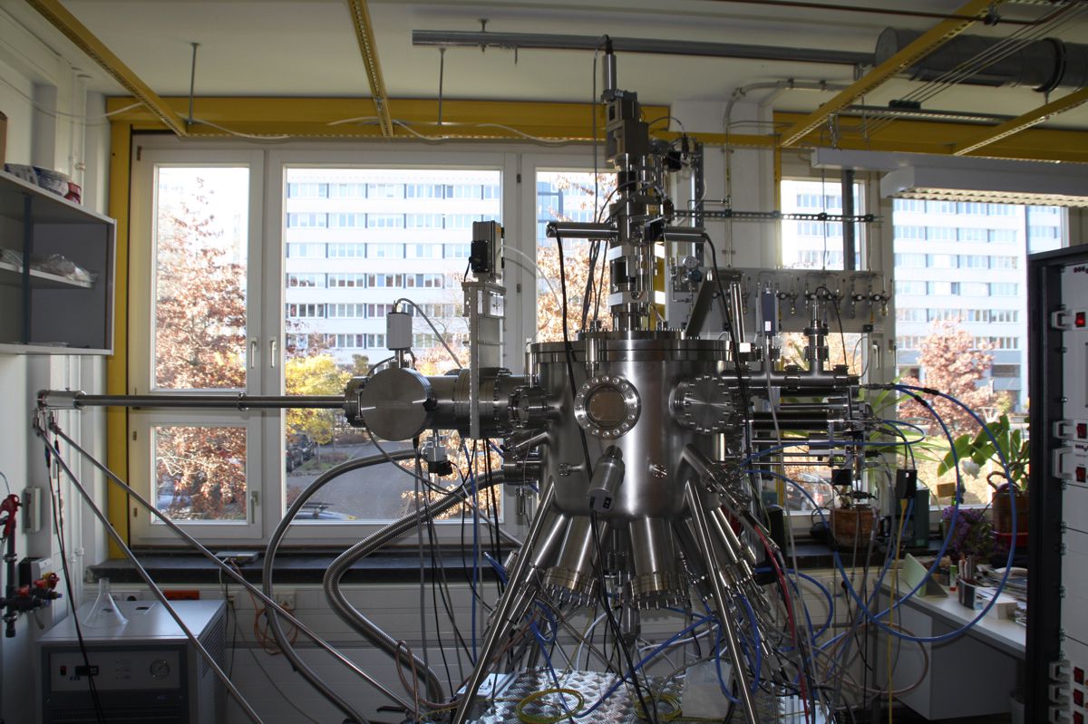
System 1: Excimerlaser (Coherent LPX Pro 305, wavelength 248 nm, pulse energy 1100 mJ, pulse repetition 50 Hz),
large-area PLD chambers for 3-inch diameter wafers, max. growth temperature 750°C, multi-target manipulator (E-, F-, W-chamber).
Photos
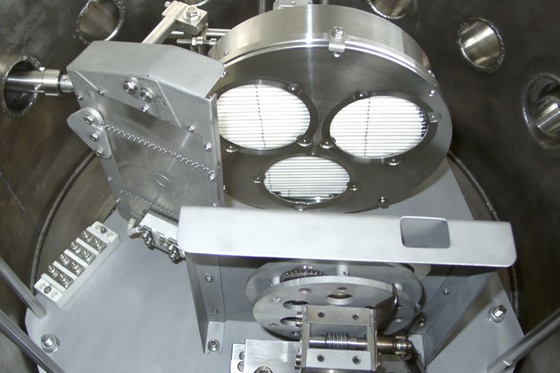
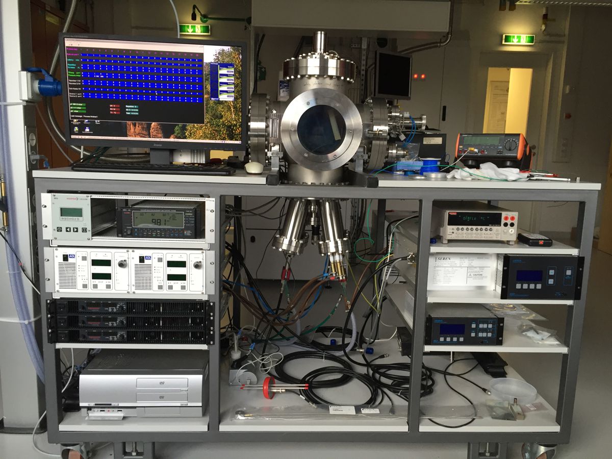
System 2: Excimerlaser (Coherent LPX Pro 305, wavelength 248 nm, pulse energy 1100 mJ, pulse repetition 50 Hz),
large-area PLD chamber for 4-inch diameter wafers, max. growth temperature 750°C, selectable multi-target manipulators for planar or cylindrical targets,
heater with tilt option for radial coating of free-standing nano- and microwires (S-chamber),
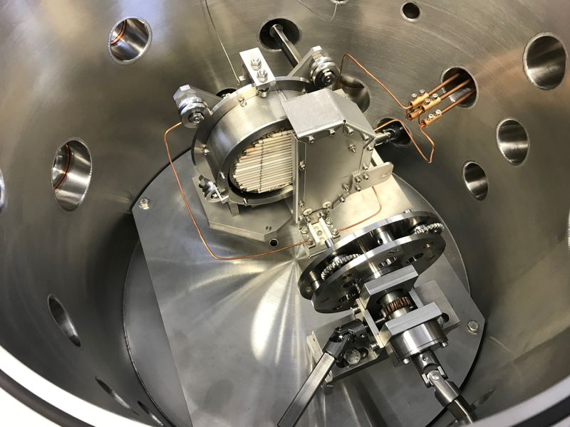
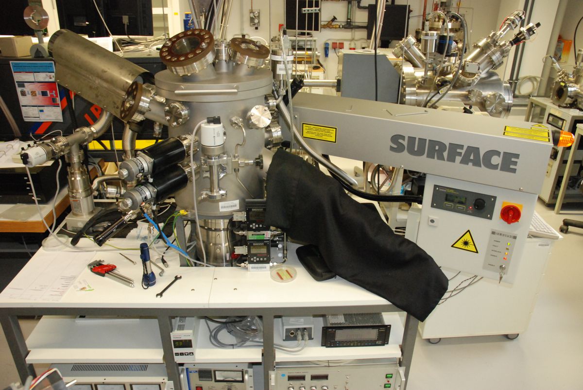
laser-MBE chamber für 10x10 mm2 substrates with in-situ RHEED (double-differentially pumped up to 0.1 mbar chamber pressure), CO2-laser
heater up to 1.400°C growth temperature (SURFACE systems), suitable for growth of nitride and oxide heterostructures (B-chamber),
high-pressure PLD chamber for nano- and microstructures, for cylindrical targets, up to 200 mbar partial pressure, heater up to 920°C (Q-chamber).
Photos
System 3: Excimerlaser (Coherent LPX Pro 305, wavelength 248 nm, pulse energy 1100 mJ, pulse repetition 50 Hz),
large-area PLD chamber for 4-inch diameter wafers, extendable up to 8-inch diameter, max. growth temperature 750°C, multi-target manipulator (G-chamber)
for combinatorial PLD (continuous composition spread PLD, CCS-PLD).
IR laser diode heated chamber (A-chamber) for combinatorial PLD (VCCS-PLD).
Photo
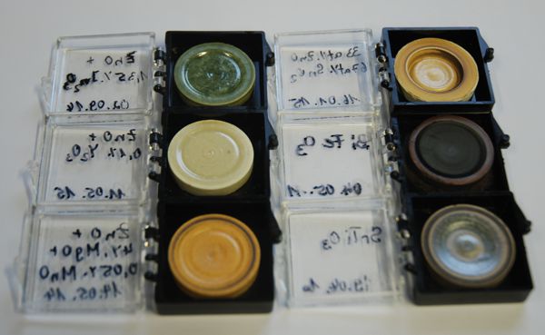
Selection of ceramic PLD targets
Key publications
M. Lorenz, H. Wei, F. Jung, S. Hohenberger, H. Hochmuth, M. Grundmann
Two-dimensional Frank - van der Merwe growth of functional oxide and nitride thin film superlattices by pulsed laser deposition
J. Mat. Res. 32, 3936 (2017) | doi
M. Lorenz, H. Hochmuth, M. Kneiß, M. Bonholzer, M. Jenderka, M. Grundmann
From high-TC superconductors to highly correlated Mott insulators - 25 years of pulsed laser deposition of functional oxides in Leipzig
Semic. Sci. Technol. 30, 024003 (2015) | doi
H. von Wenckstern, Z. Zhang, F. Schmidt, J. Lenzner, H. Hochmuth, M. Grundmann
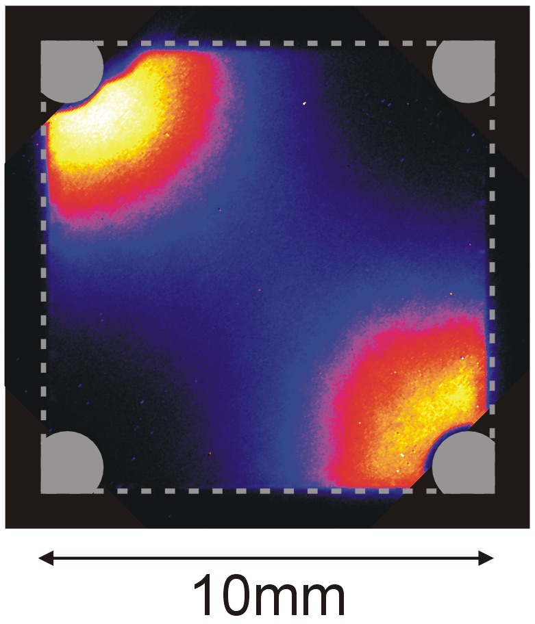
Continuous composition spread using pulsed-laser deposition with a single, segmented target
CrystEngComm 15, 10020 (2013) | doi
M. Kneiß, P. Storm, G. Benndorf, M. Grundmann, H. von Wenckstern
Combinatorial material science and strain engineering enabled by pulsed laser deposition using radially segmented targets
ACS Comb. Sci. 20, 643 (2018) | doi
|
More on sputter deposition
|
Sputter system from MANTIS for deposition of amorphous metal oxides and oxynitrides and reactively sputtered Schottky contacts (PtOx, PdOx, ...).
Photo
Key publications
S. Müller, H. von Wenckstern, F. Schmidt, D. Splith, H. Frenzel, M. Grundmann
Method of choice for fabrication of high-quality β-gallium oxide-based Schottky diodes
Semic. Sci. Technol. 32, 065013 (2017) | doi
A. Reinhardt, H. Frenzel, H. von Wenckstern, D. Spemann, M. Grundmann
Electron transport mechanism in rf-sputtered amorphous zinc oxynitride thin films
phys. stat. sol. (a) 213, 1767 (2016) | doi
H. Frenzel, T. Dörfler, P. Schlupp, H. von Wenckstern, M. Grundmann
Long-throw magnetron sputtering of amorphous Zn-Sn-O-thin films at room temperature
phys. stat. sol. (a) 212, 1482 (2015) | doi
Home-built sputter system for deposition of metal halogen semiconductors, such as copper iodide and related materials.
Photo
Key publications
C. Yang, D. Souchay, M. Kneiß, M. Bogner, H. M. Wei, M. Lorenz, O. Oeckler, G. Benstetter, Y.Q. Fu, M. Grundmann
Transparent Flexible Thermoelectric Material Based on Non-toxic Earth-Abundant p-Type Copper Iodide Thin Film
Nature Commun. 8, 16076 (2017) | doi
C. Yang, M. Kneiß, F.-L. Schein, M. Lorenz, M. Grundmann
Room-temperature domain-epitaxy of copper iodide thin films for transparent CuI/ZnO heterojunctions with high rectification ratios larger than 109
Sci. Rep. 6, 21937 (8 pages) (2016) | doi
|
More on plasma-enhanced chemical vapor deposition
|
|
Photo
Key publication
R. Schmidt-Grund, T. Nobis, V. Gottschalch, B. Rheinländer, H. Herrnberger, M. Grundmann
a-Si/SiOx Bragg-reflectors on micro-structured InP
Thin Solid Films 483, 257 (2005) | doi
|
More on thermal evaporation
|
|
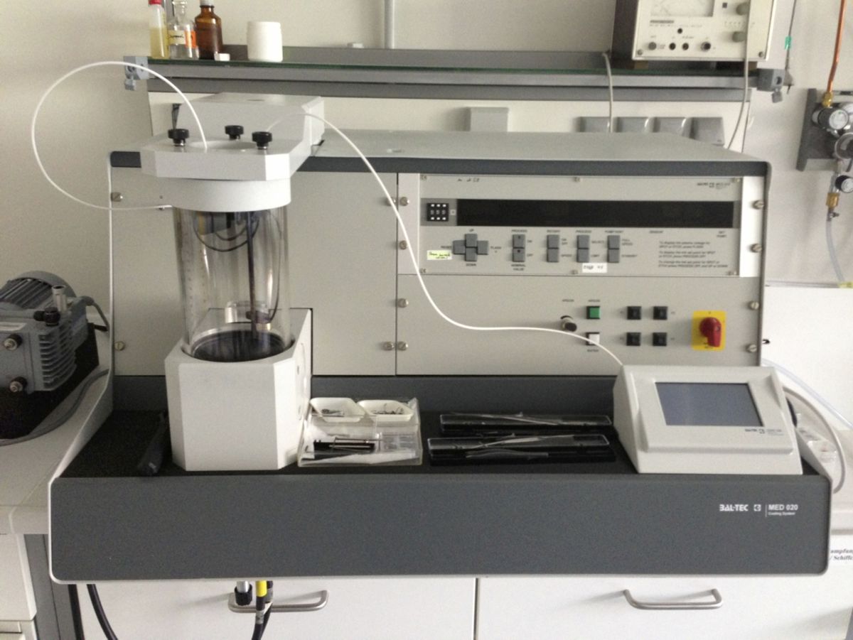
BALTEC MED 020
Photo
|
More on carbo-thermal evaporation
|
|
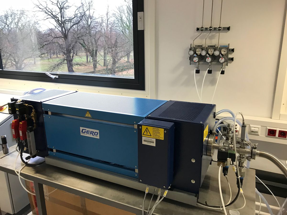
GERO tube furnace F 70-500, up to 1350°C
Photo
Key publication
B. Cao, M. Lorenz, M. Brandt, H. von Wenckstern, J. Lenzner, G. Biehne, M. Grundmann
p-type conducting ZnO:P microwires prepared by direct carbothermal growth
phys. stat. sol. RRL 2, 37 (2008) | doi
|
More on thermal annealing
|
|
Photo
|
|
| |
|
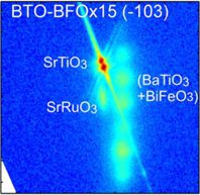
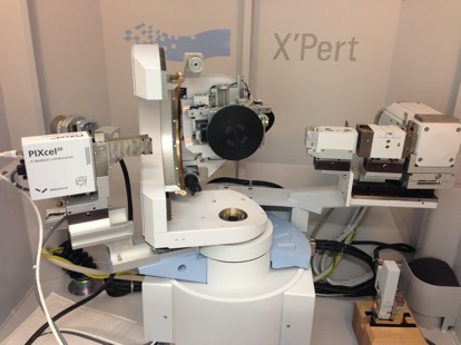
Structural Characterization
Structural characterization is the first step after sample fabrication in order to understand the crystal phase, lattice constants and strain state of the thin films. Also surface roughness or complex morphology such as nanowire arrays or circuit patterns are important properties that are analyzed.
More on X-ray diffraction
|
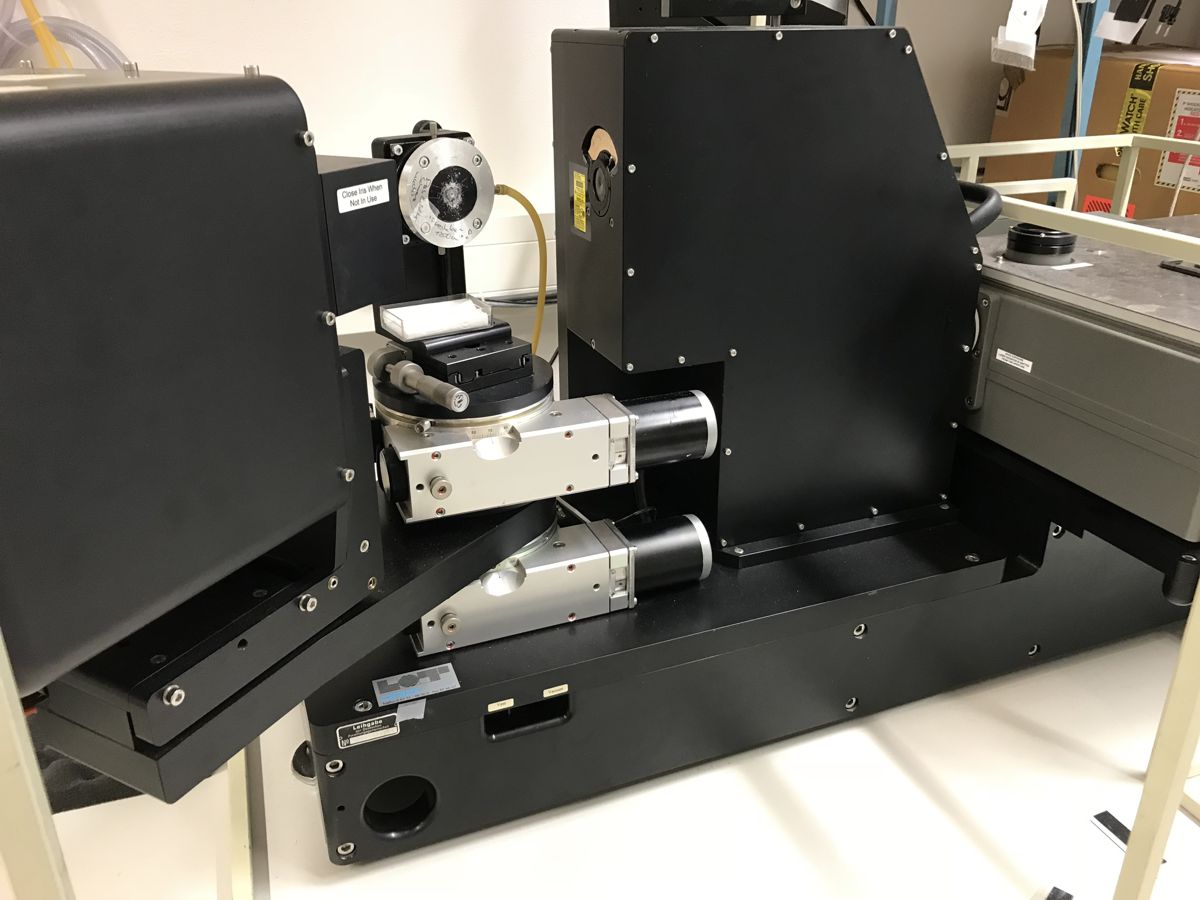
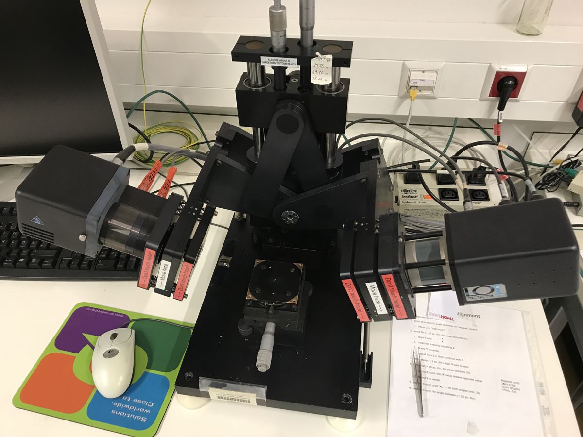
PANalytical X'pert PRO materials research diffractometer for XRD, high-resolution XRD, X-ray reflectivity;
with PIXcel3D array detector, four-circle high precision goniometer, modular optics.
Photo
Key publications
H. Wei, M. Grundmann, M. Lorenz
Confinement-driven metal-insulator transition and polarity-controlled conductivity of epitaxial LaNiO3/LaAlO3 (111) superlattices
Appl. Phys. Lett. 109, 082108 (2016) | doi
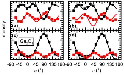
M. Grundmann, M. Scheibe, M. Lorenz, J. Bläsing, A. Krost
X-ray multiple diffraction of ZnO substrates and heteroepitaxial thin films
phys. stat. sol. (b) 251, 850 (2014) | doi
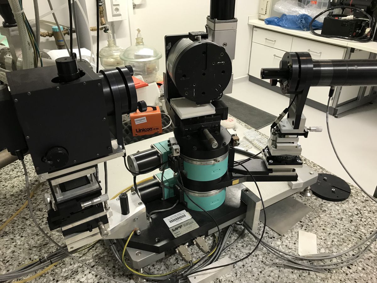
X-ray diffractometer Philips X'pert with wide-angle Bragg-Brentano goniometer with secondary graphite monochromator, and with high-resolution (triple-axis) goniometer with 4 x Ge(220) monochromator.
|
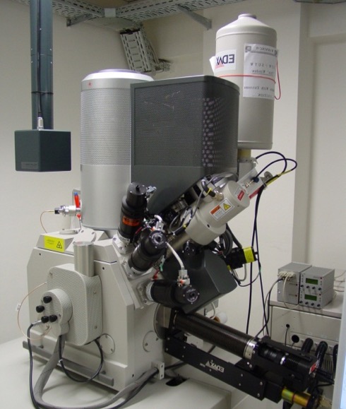
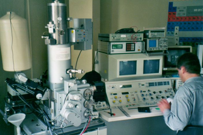
More on scanning electron microscopy
|
Field emission gun scanning electron microscope (FEI Nanolab 200) with focussed
ion beam for high resolution SEM imaging, preparation of cross-sections and TEM lamellae.
Photo
Key publications
S. Müller, H. von Wenckstern, O. Breitenstein, J. Lenzner, M. Grundmann
Microscopic identification of hot spots in multi-barrier Schottky contacts on pulsed laser deposition grown zinc oxide thin films
IEEE Transact. Electr. Dev. 59, 536 (2012) | doi
C. Sturm, H. Hilmer, R. Schmidt-Grund, M. Grundmann
Observation of strong exciton-photon coupling at temperatures up to 410 K
New J. Phys. 11, 073044 (2009) | doi
|
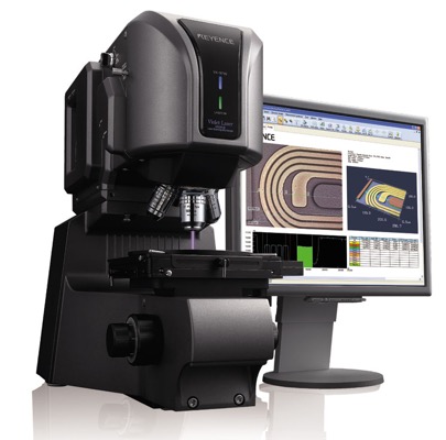
More on laser scanning microscopy
|
Confocal laser scanning microscope (KEYENCE VK-X 210) with 16 bit photomultiplier,
laser differential-interference contrast, with automatic XY-image composition (stitching).
Photo
|
More on atomic force microscopy
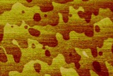
|
Scanning probe microscope (Park XE-150) for atomic force microscopy (AFM), scanning tunneling microscopy (STM), piezo force microscopy (PFM), magnetic force microscopy (MFM), scanning capacitance microscopy (SCM), variable enhanced conductive AFM, scanning spread resistance (SSRM), Kelvin probe force microscopy (KPFM), nanoindentation.
Photo
Key publications
M. Bonholzer, M. Lorenz, M. Grundmann
Layer-by-layer growth of TiN by pulsed laser deposition on in-situ annealed (100) MgO substrates
phys. stat. sol. (a) 211, 2621 (2014) | doi
|
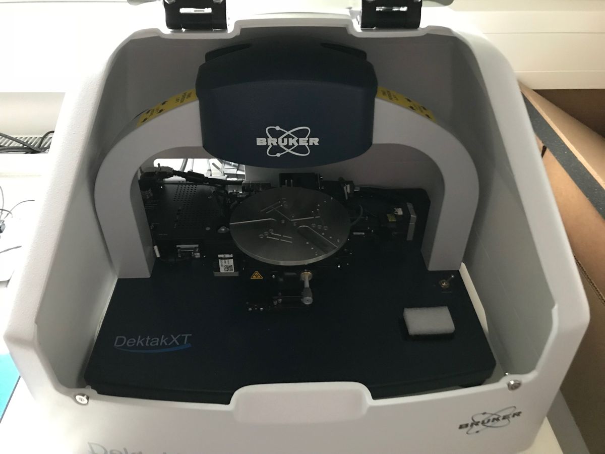
More on profilometer
|
|
Stylus profiler (Bruker Dektak XT) for 2D roughness surface characterization, and step height
measurements, and advanced 3D mapping and film stress analyses.
Photo
|
|
| |
|
Electrical Characterization
The measurement and understanding of electrical properties is essential for the design and modelling of electronic devices. For this purpose we entertain various methods to investigate electrical properties such as conductivity, carrier density, carrier mobility, and impedance. Typically frequency- and temperature-dependent investigations are made for conclusive analysis. The results also give a feedback to sample fabrication for optimized doping schemes.
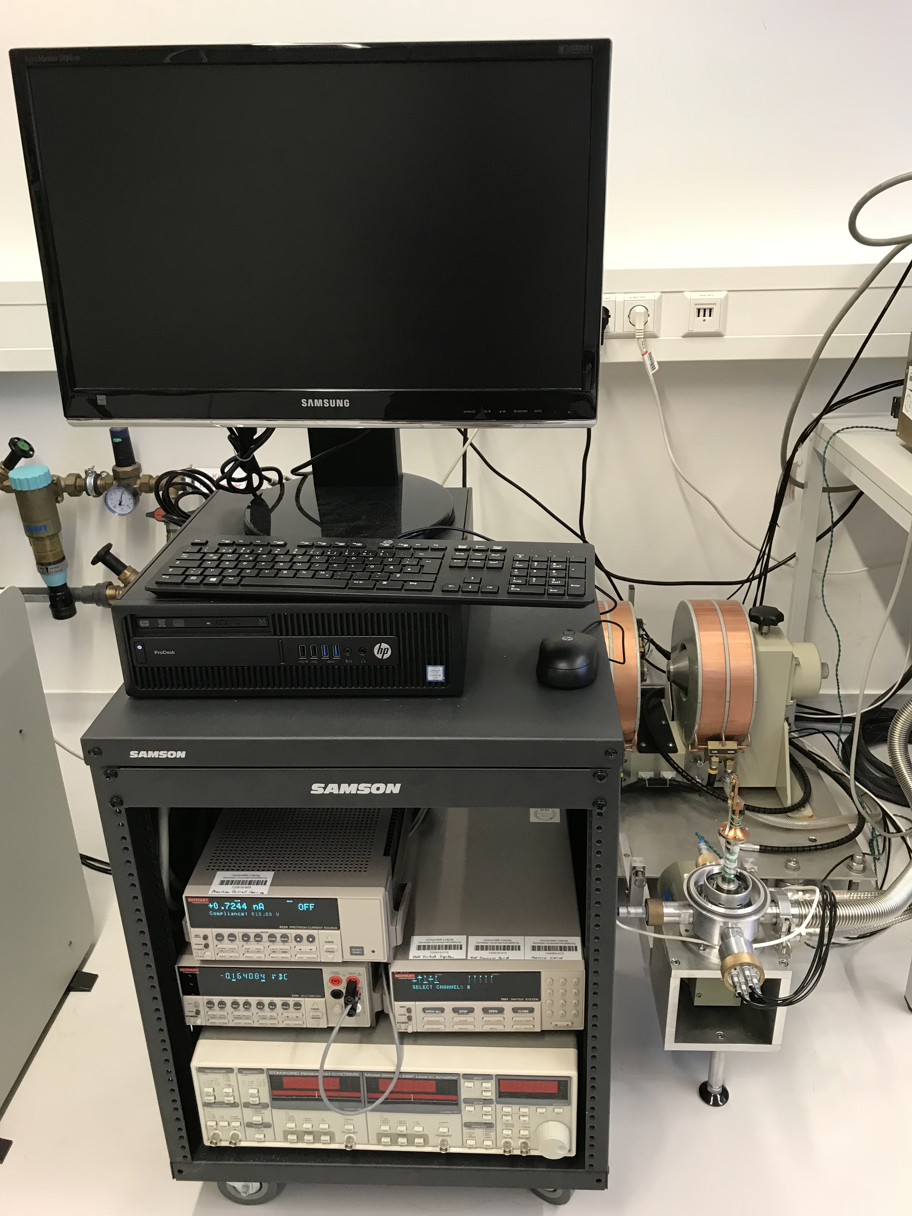
More on IV and CV characterization
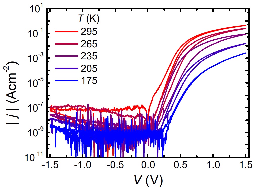
|
Current-voltage and capacitance-voltage spectroscopy, also as a function of temperature.
Photos
Key publications
S. Bitter, P. Schlupp, H. von Wenckstern, M. Grundmann
The Vital Role of Oxygen for the Formation of Highly Rectifying Schottky Barrier Diodes on Amorphous Zinc-Tin-Oxide with Various Cation Composition
ACS Appl. Mater. Interfaces 9, 26574 (2017) | doi
Daniel Splith, Stefan Müller, Florian Schmidt, Holger von Wenckstern, Johan Janse van Rensburg, Walter E. Meyer, Marius Grundmann
Determination of the mean and the homogeneous barrier height of Cu Schottky contacts on heteroepitaxial β-Ga2O3 thin films grown by pulsed laser deposition
phys. stat. sol. (a) 211, 40 (2014) | doi
|
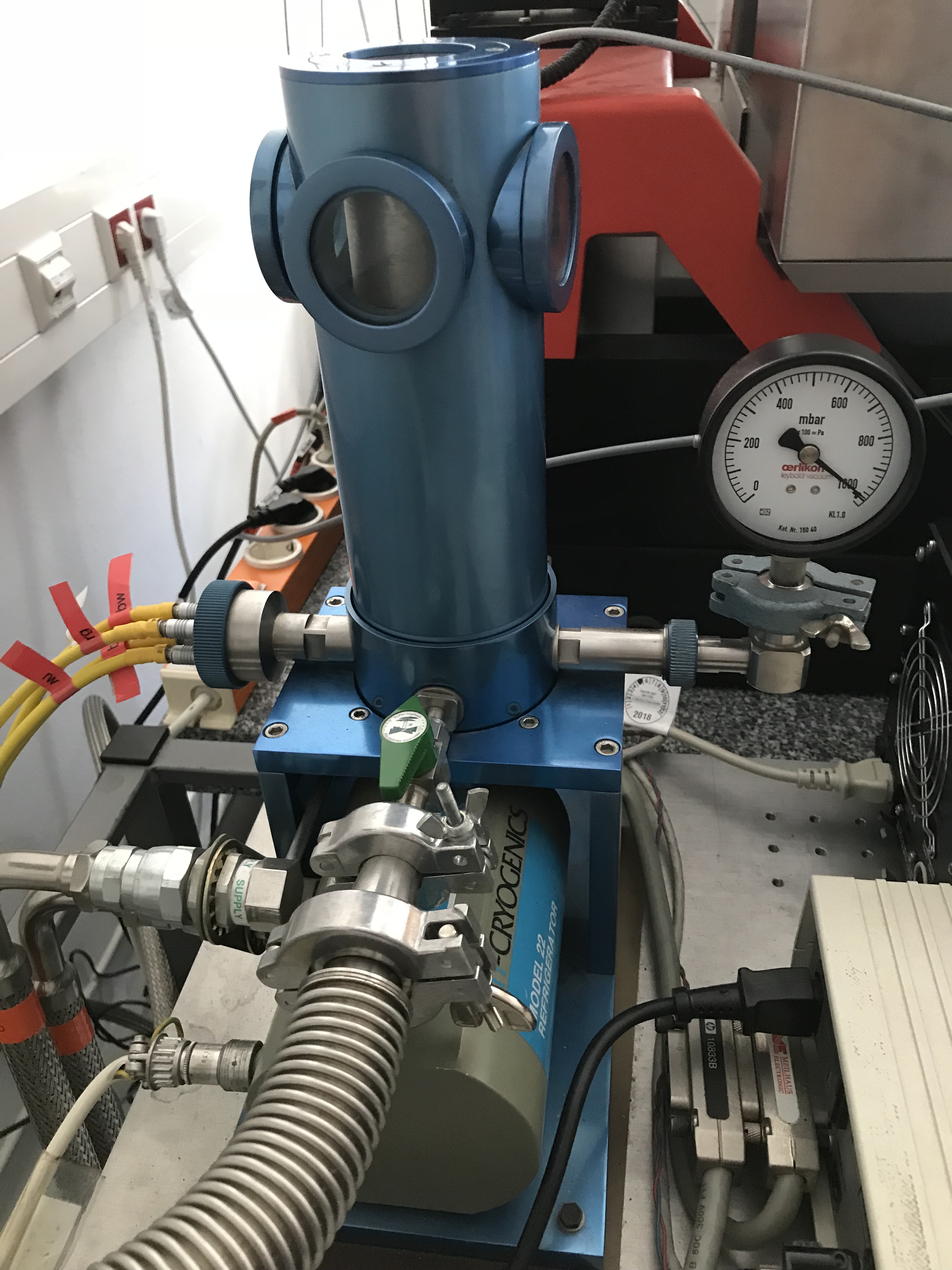
More on Hall effect
|
Temperature-dependent Hall effect for the measurement of carrier density and mobility (and carrier type from sign of Hall effect). Evaluation with single and double channel models and quantitative mobility spectrum analysis.
Hall effect (max. 0.43 T, 35-300 K, 300-700 K),
Hall effect (max. 1 T, 20-300 K),
Photos
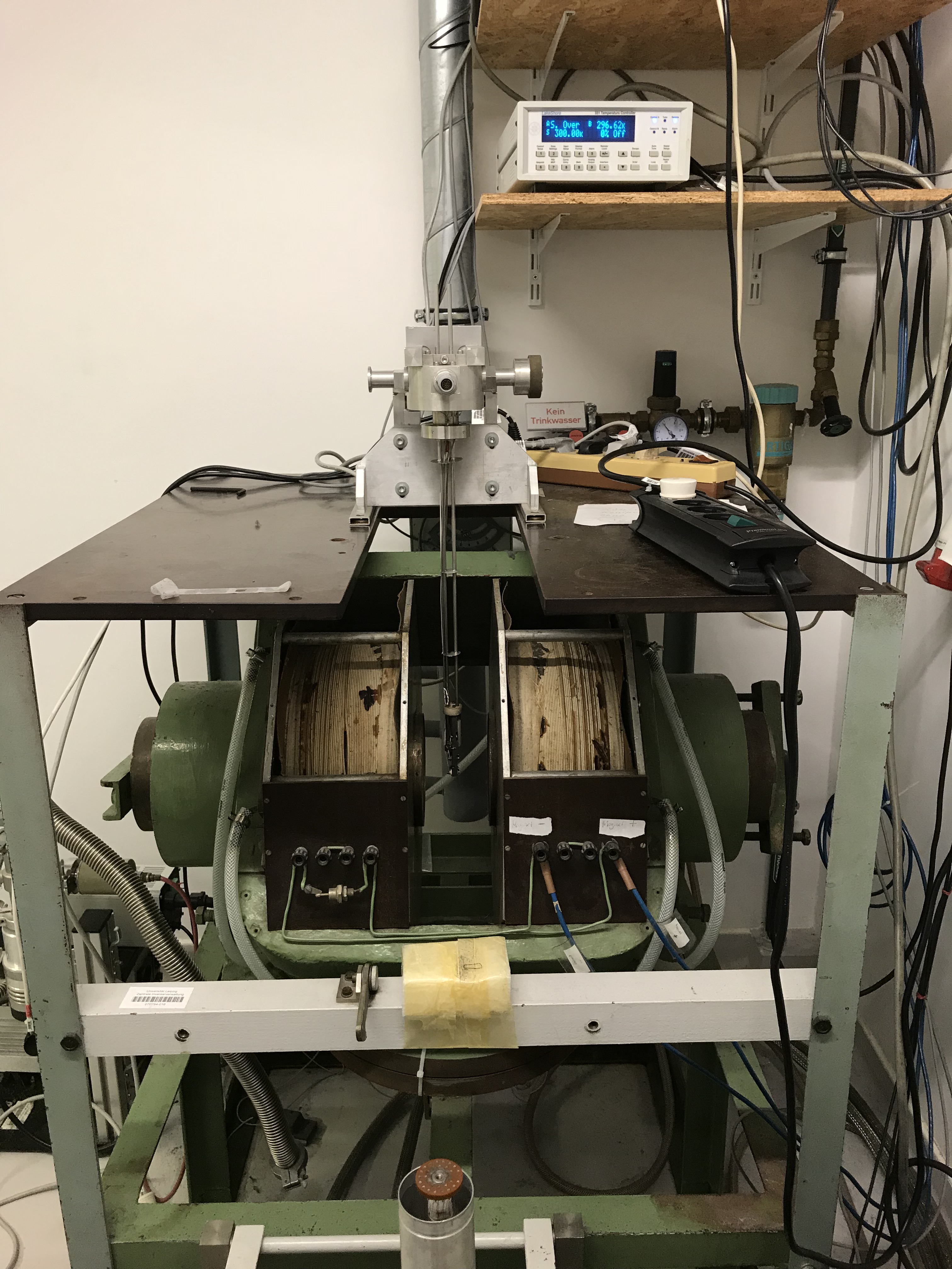
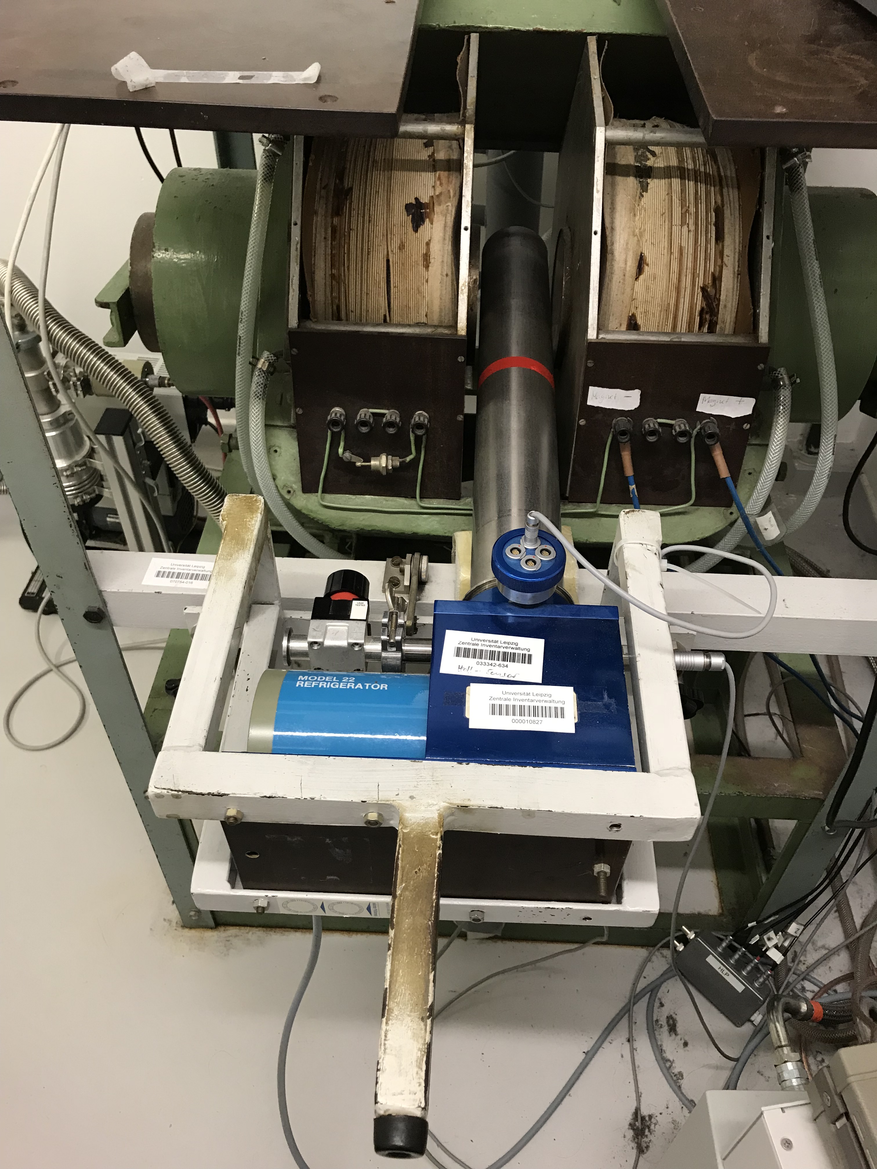
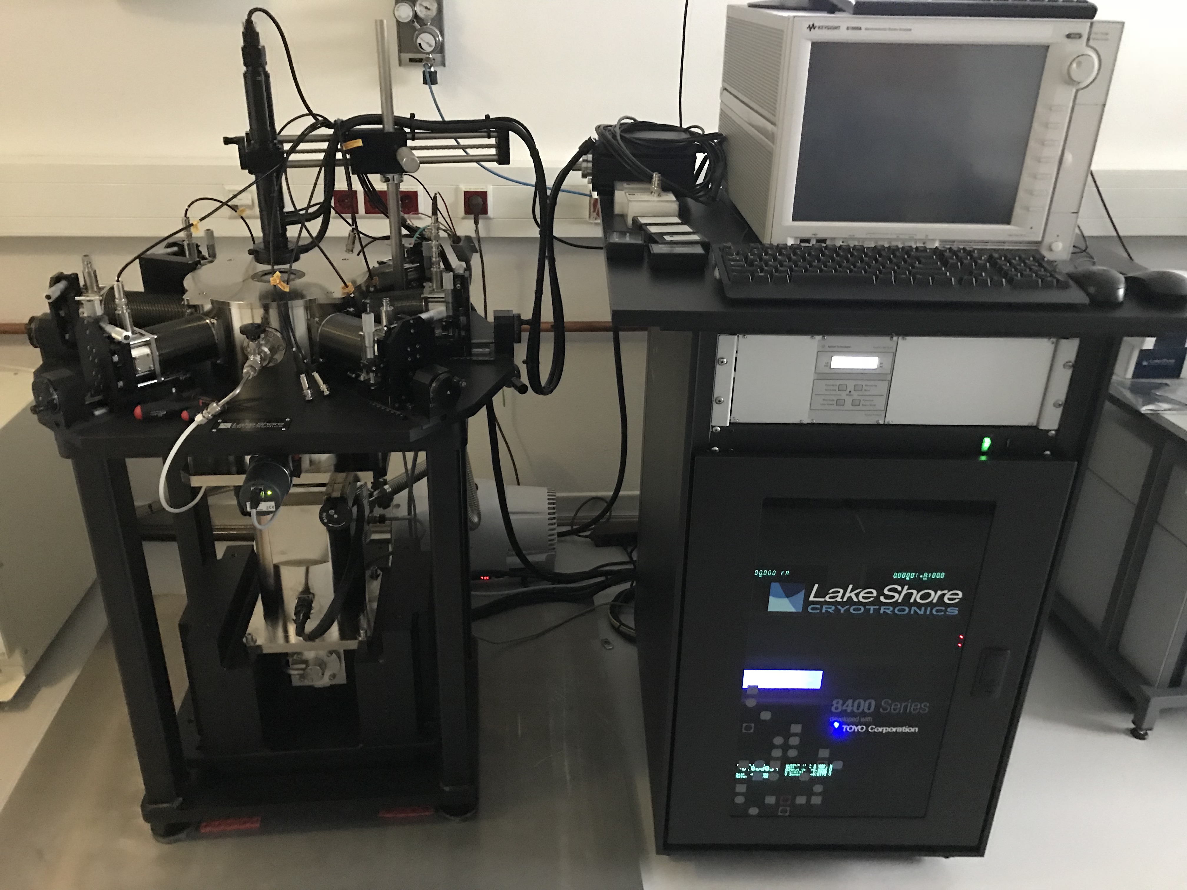
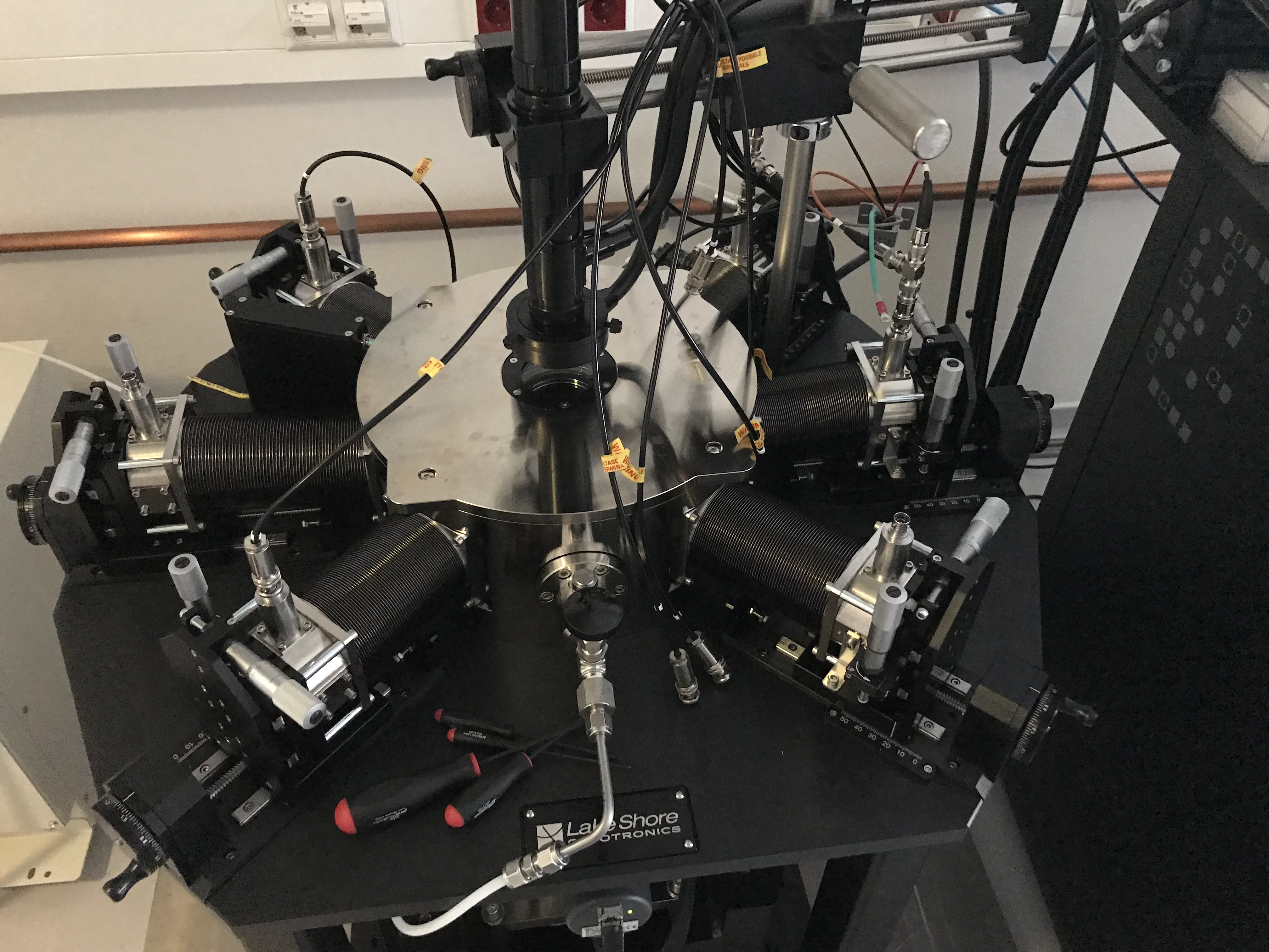
Micro-Hall effect wafer prober (Lakeshore 8425 with cryogenic probes) (max. 2 T, 4.2-400 K)
Photos
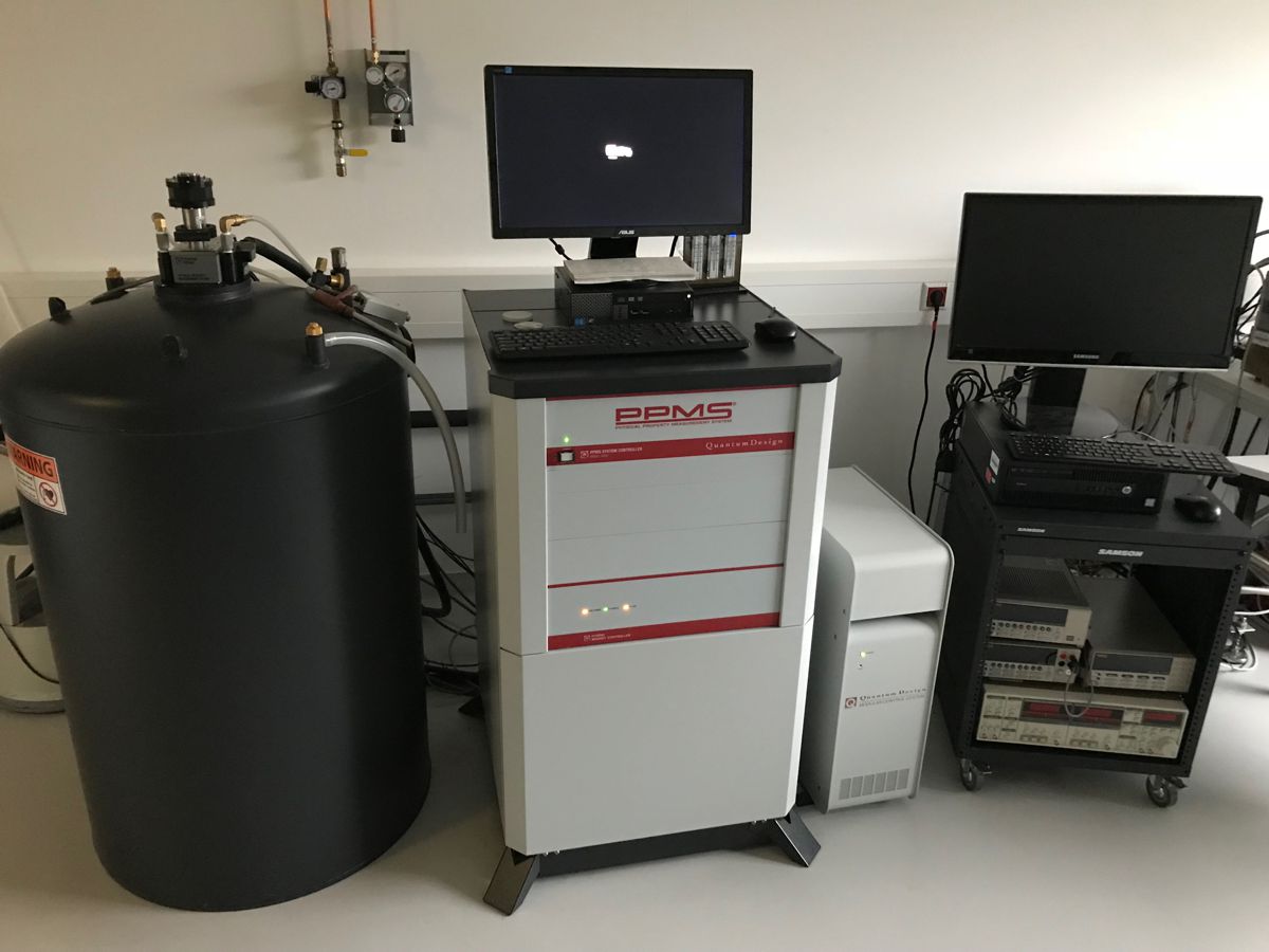
Physical property measurement system (PPMS-9, Quantum Design) (max. 9 T, 1.9-400 K),
Photo
Key publications
M. Brandt, H. von Wenckstern, H. Schmidt, A. Rahm, G. Biehne, G. Benndorf, H. Hochmuth, M. Lorenz, Ch. Meinecke, T. Butz, M. Grundmann
High electron mobility of phosphorous doped homoepitaxial ZnO thin films grown by pulsed laser deposition
J. Appl. Phys. 104, 013708 (2008) | doi
E. M. Kaidashev, M. Lorenz, H. von Wenckstern, J. Lenzner, G. Benndorf, A. Rahm, H.-C. Semmelhack, K.-H. Han, H. Hochmuth, C. Bundesmann, V. Riede, M. Grundmann
High electron mobility of epitaxial ZnO thin films on c-plane sapphire grown by multistep pulsed-laser deposition
Appl. Phys. Lett. 82, 3901 (2003) | doi
|
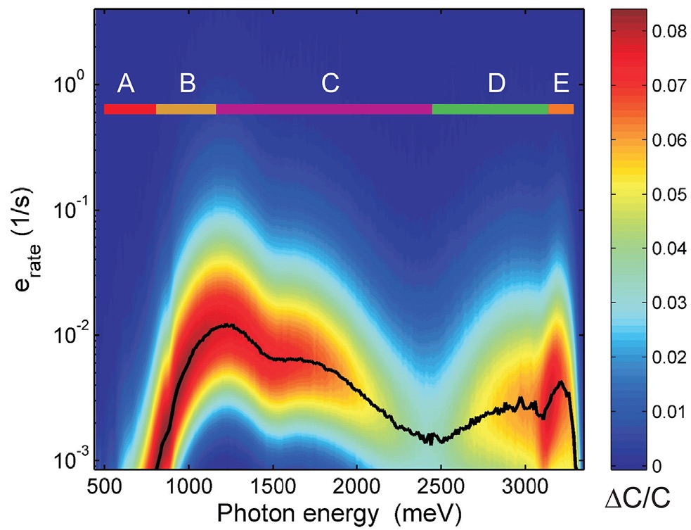
More on thermal admittance spectroscopy (TAS)
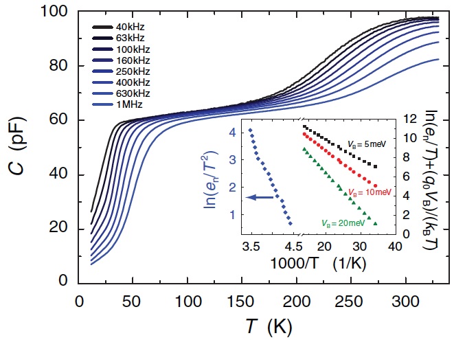
|
TAS is the determination of the temperature-dependent impedance (in particular capacitance) for various
frequencies. The evaluation yields the electronic levels of shallow defects.
Key publication
H. von Wenckstern, D. Splith, F. Schmidt, M. Grundmann, O. Bierwagen, J.S. Speck
Schottky contacts to In2O3
APL Mater. 2, 046104 (2017) | doi
|
More on deep level transient spectroscopy (DLTS/ODLTS)
|
Key publications
Rainer Pickenhain, Matthias Schmidt, Holger von Wenckstern, Gabriele Benndorf, Andreas Pöppl, Rolf Böttcher, Marius Grundmann
Negative U Properties of the Deep Level E3 in ZnO
phys. stat. sol. (b) 255, 1700670 (2018) | doi
F. Schmidt, H. von Wenckstern, O. Breitenstein, R. Pickenhain, M. Grundmann
Low Rate Deep Level Transient Spectroscopy: A powerful tool for defect characterization in wide bandgap semiconductors
Solid State Electr. 92, 40 (2014) | doi
|
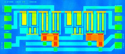
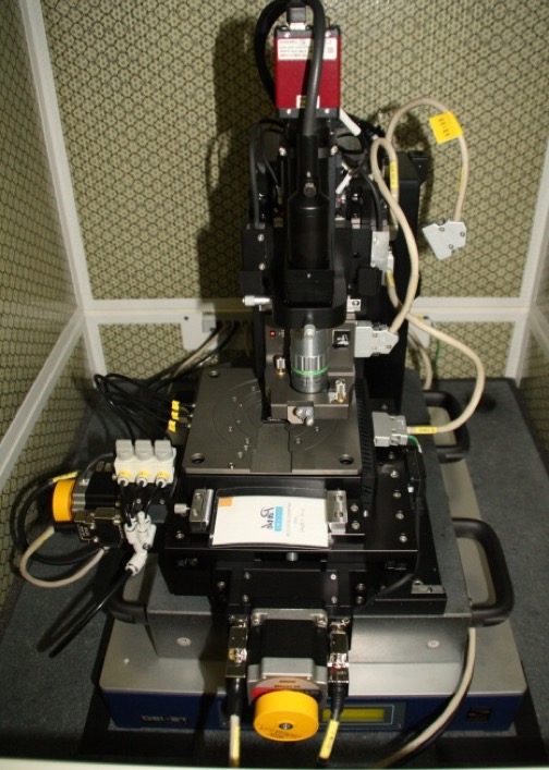
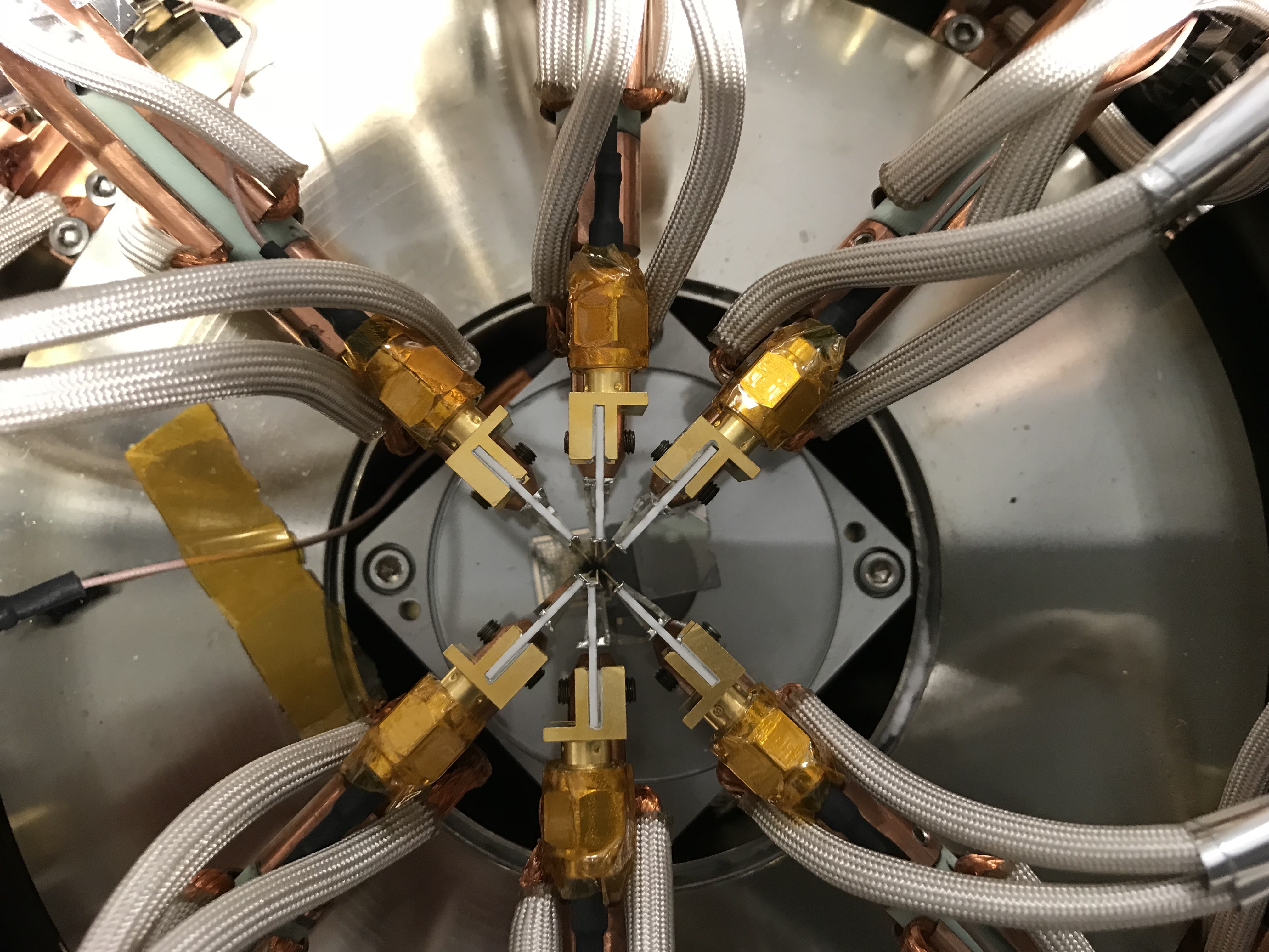
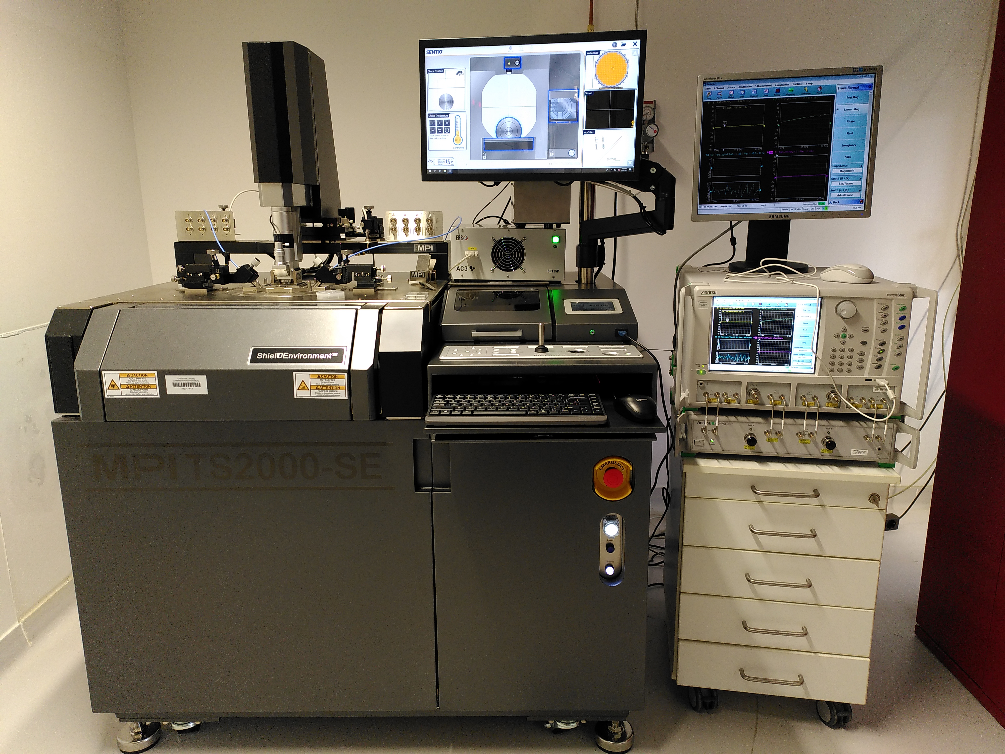
More on wafer probing
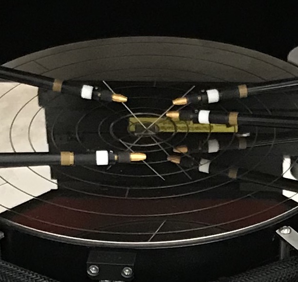
|
Semiautomatic wafer prober
Photo
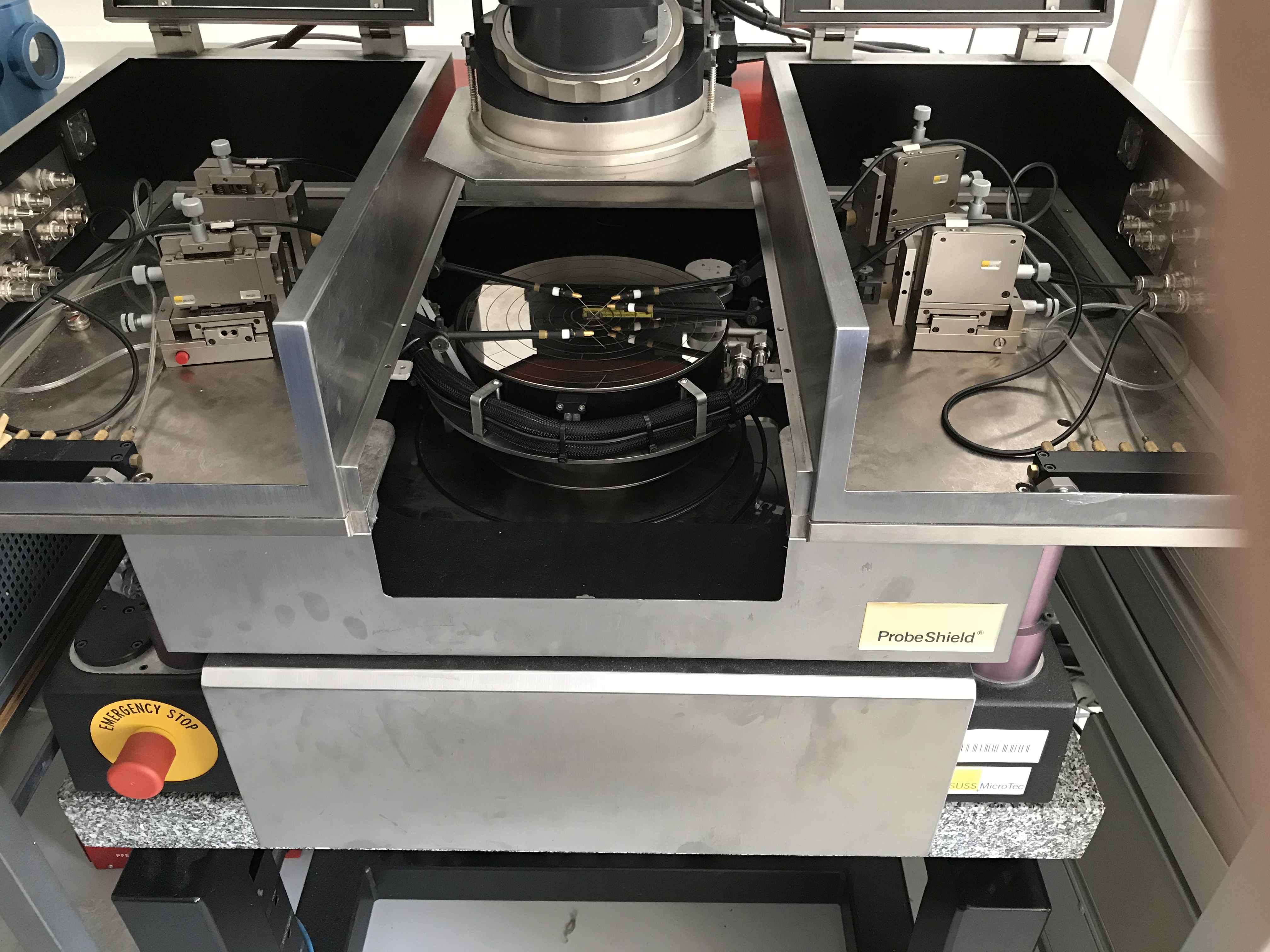
HF wafer prober
Photo
|
|
| |
|
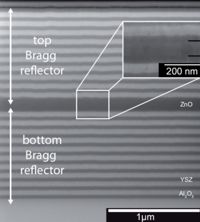
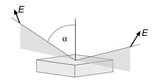
Optical Characterization
The characterization of optical properties of bulk material, thin films and nanostructures concerns
the determination of the complex dielectric function tensor with spectroscopic ellipsometry, the phonon modes
with Raman spectroscopy, and recombination properties using photoluminescence with spectral,
spatial, angular, polarization and time resolution. Also cathodoluminescence is used for hyper-spectral
imaging of thin films, nano- and microstructures. All methods can be recorded as a function of temperature.
More on spectroscopic ellipsometry
|
Generalized, spectroscopic ellipsometry from MIR to VUV spectral ranges (0.04-9 eV), in particular for optically
anisotropic materials, Bragg mirrors, oxide heterostructures and combinatorial gradient samples.
VUV ellipsometer (Woollam VUV-VASE Gen II, 0.14-2.4 μm)
Photo
Key publications
C. Sturm, R. Schmidt-Grund, V. Zviagin, M. Grundmann
Temperature dependence of the dielectric tensor of monoclinic dielectric Ga2O3 single crystals in the spectral range 0.5-8.5 eV
Appl. Phys. Lett. 111, 082102 (2017) | doi
C. Sturm, J. Furthmüller, F. Bechstedt, R. Schmidt-Grund, M. Grundmann
Dielectric tensor of monoclinic Ga2O3 single crystals in the spectral range 0.5-8.5 eV
APL Mater. 3, 106106 (2015) | doi
Full Müller matrix ellipsometer (Woollam RC2-D+NIR, 0.19-1.69 μm, 1088 wavelenghts)
Photo
Key publications
C. Sturm, S. Höfer, K. Hingerl, T.G. Mayerhöfer, M. Grundmann
Dielectric function decomposition by dipole orientation distribution: Application to triclinic K2Cr2O7
New J. Phys. 22, 073041 (2020) | doi
C. Sturm, V. Zviagin, M. Grundmann
Dielectric tensor, optical activity and singular optic axes of KTP in the spectral range 0.5-8.4 eV
Phys. Rev. Mater. 4, 055203 (2020) | doi
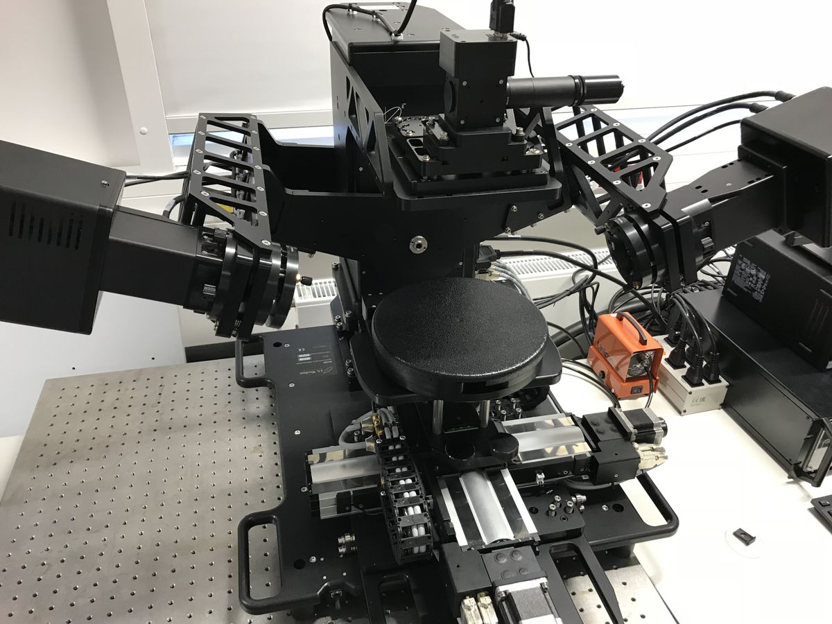
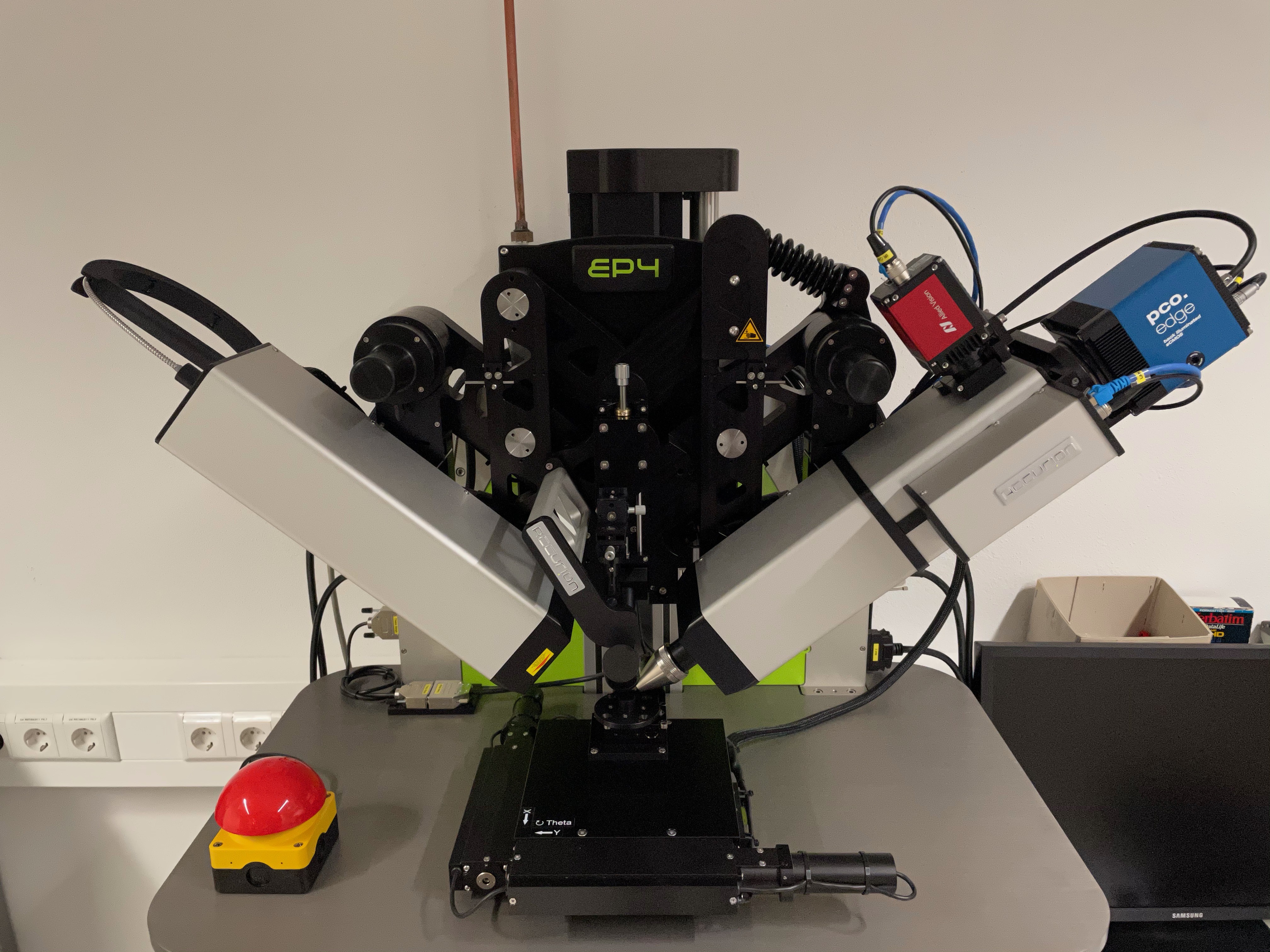
Imaging ellipsometer (Accurion ep4, 0.19-1.70 μm)
Photo
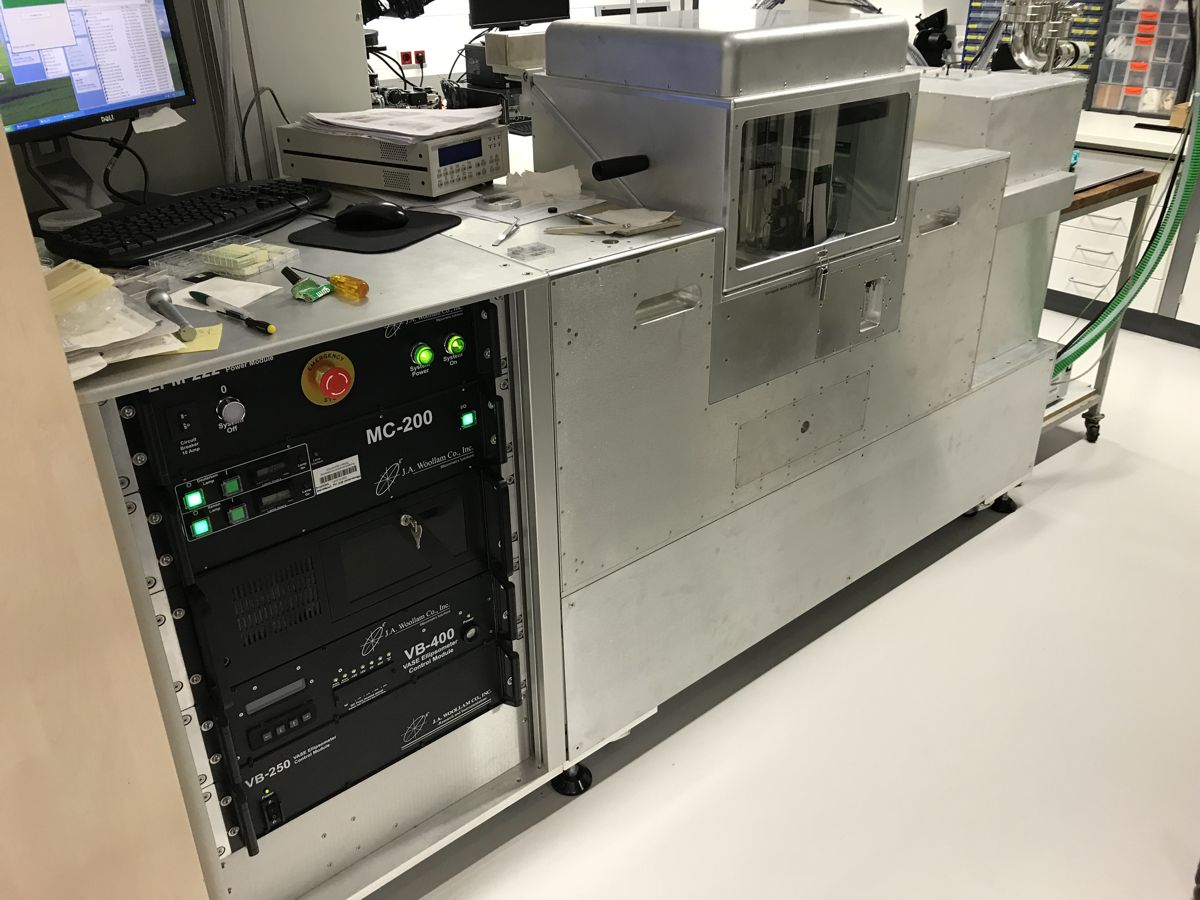
UV-VIS-NIR ellipsometer (Woollam VASE, 0.24-1.70 μm)
Photo
Key publication
J. Sellmann, C. Sturm, R. Schmidt-Grund, C. Czekalla, J. Lenzner, H. Hochmuth, B. Rheinländer, M. Lorenz, M. Grundmann
Structural and optical properties of ZrO2 and Al2O3 thin films and Bragg reflectors grown by pulsed laser deposition
phys. stat. sol. (c) 5, 1240-1243 (2008) | doi
FTIR ellipsometer (Woollam IR-VASE, 2-30 μm)
Photo
Key publication
C. Bundesmann, A. Rahm, M. Lorenz, M. Grundmann, M. Schubert
Infrared optical properties of MgxZn1-xO thin films (0≤x≤1): Long-wavelength optical phonons and dielectric constants
J. Appl. Phys. 99, 113504 (2006) | doi
UV-VIS-NIR multi-channel ellipsometer (Woollam M2000, 0.36-1.70 μm, 512 wavelengths)
Photo
|
More on Raman scattering
|
(Micro-) Raman spectroscopy with 532, 355, 325 and 266 nm excitation, U1000 double monochromator and LN2-cooled
CCD detector, UV microscopy and polarization optics. In particular determination of the Raman tensor of optically uniaxial and biaxial crystals
considering birefringent effects.
Photo
Key publications
C. Kranert, C. Sturm, R. Schmidt-Grund, M. Grundmann
Raman Tensor Formalism for Optically Anisotropic Crystals
Phys. Rev. Lett. 116, 127401 (2016) | doi
C. Kranert, C. Sturm, R. Schmidt-Grund, M. Grundmann
Raman tensor elements of β-Ga2O3
Sci. Rep. 6, 35964 (2016) | doi
C. Kranert, M. Jenderka, J. Lenzner, M. Lorenz, H. von Wenckstern, R. Schmidt-Grund, M. Grundmann
Lattice parameters and Raman-active phonon modes of β-(AlxGa1-x)2O3
J. Appl. Phys. 117, 125703 (2015)| doi
|
More on photoluminescence (PL)
|
Photoluminescence is used to investigate radiative recombination channels in various materials
and structures.
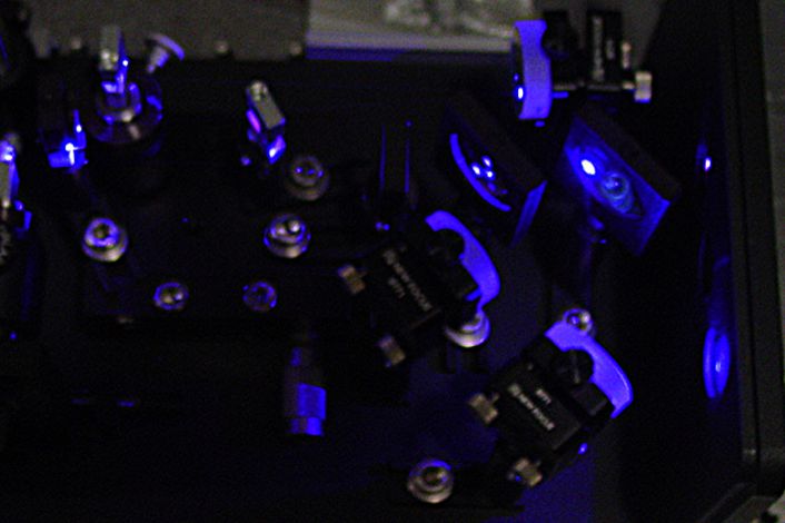
cw-photoluminescence using various lasers, e.g. HeCd (325 nm), for excitation without particular
spatial resolution. Spectra are detected using various photomultipliers (GaAs, MCP) and CCDs and are
recorded as a function of excitation density and temperature.
Photo
Key publications
C.P. Dietrich, M. Lange, G. Benndorf, J. Lenzner, M. Lorenz, M. Grundmann
Competing exciton localization effects due to disorder and shallow defects in semiconductor alloys
New J. Phys. 12, 033030 (2010) | doi
M. Lange, C.P. Dietrich, K. Brachwitz, T. Böntgen, M. Lorenz, M. Grundmann
(Zn,Cd)O thin films for the application in heterostructures: structural and optical properties
J. Appl. Phys. 112, 103517 (2012) | doi
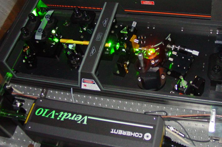
Time-resolved photoluminescence using a fs Ti:Sa laser (Coherent VERDI-10, Coherent MIRA-F, APE Pulse Select,
U-Oplaz TP-2000B SHG/THG) for excitation and single photon counting (Hamamatsu MCP-PM) for detection.
Photo
Key publications
A. Müller, M. Grundmann
Tunneling dynamics of excitons in random semiconductor alloys
Phys. Rev. B 87, 035134 (2013) | doi
M. Stölzel, A. Müller, G. Benndorf, M. Brandt, M. Lorenz, M. Grundmann
Determination of unscreened exciton states in polar ZnO/(Mg,Zn)O quantum wells with strong quantum-confined Stark effect
Phys. Rev. B 88, 045315 (2013) | doi
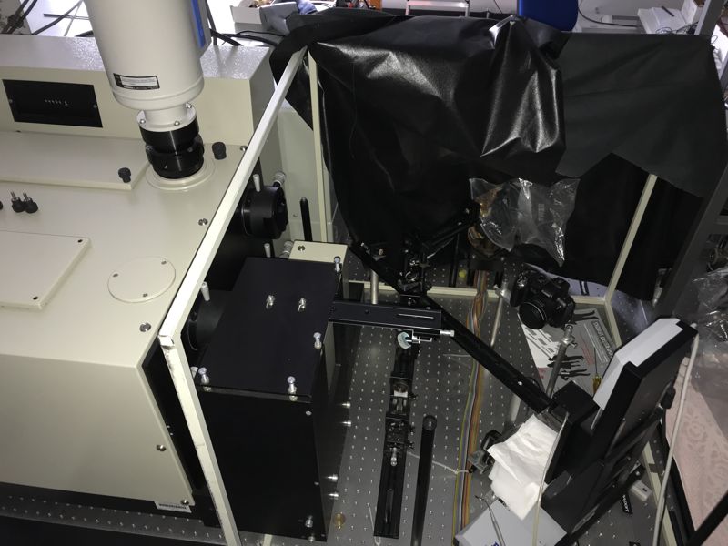
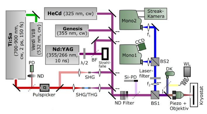
Micro-photoluminescence using various cw- and fs-lasers for excitation with high, diffraction-limited spatial resolution. Spectra
can be recorded angularly resolved (Fourier imaging) and time-resolved with a streak camera (Hamamatsu C5680/Jobin-Yvon iHR320).
Photo
Key publications
C.P. Dietrich, M. Lange, C. Sturm, R. Schmidt-Grund, M. Grundmann
One- and two-dimensional cavity modes in ZnO microwires
New J. Phys. 13, 103021 (2011) | doi
H. Franke, C. Sturm, R. Schmidt-Grund, G. Wagner, M. Grundmann
Ballistic propagation of exciton-polariton condensates in a ZnO-based microcavity
New J. Phys. 14, 013037 (2012) | doi
Optical pumping using fs- (Ti:Sa, Coherent VERDI-18, Coherent MIRA-HP, APE Pulse Select, U-Oplaz TP-2000B SHG/THG)
and ns- (SpitLight Compact DPSS, Innolas, >2 mJ/100Hz, 266/355 nm) lasers for the investigation of lasing phenomena.
Key publications
M. Wille, E. Krüger, S. Blaurock, V. Zviagin, R. Deichsel, G. Benndorf, L. Trefflich, V. Gottschalch,
H. Krautscheid, R. Schmidt-Grund, M. Grundmann
Lasing in cuprous iodide microwires
Appl. Phys. Lett. 111, 031105 (2017) | doi
M. Wille, C. Sturm, T. Michalsky, R. Röder, C. Ronning, R. Schmidt-Grund, M. Grundmann
Carrier density driven material dynamics of lasing ZnO Nanowires
Nanotechnology 27, 225702 (2016) | doi
|
More on cathodoluminescence (CL)
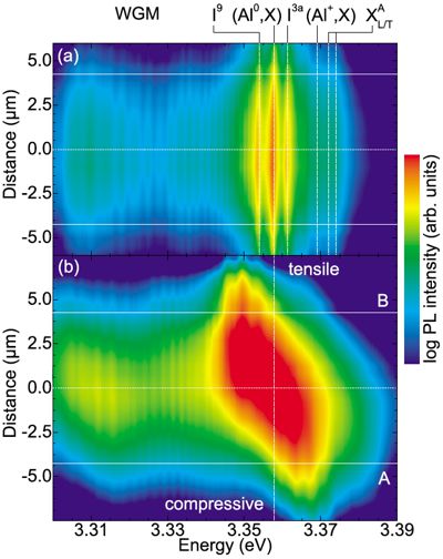
|
Cathodoluminescence is used to image lateral variations of the emission spectrum in
thin films, micro- and nanostructures. The sample temperature can be varied from liquid helium
up to room temperature.
Photo
Key publications
C.P. Dietrich, M. Lange, F.J. Klüpfel, H. von Wenckstern, R. Schmidt-Grund, M. Grundmann
Strain distribution in bent ZnO microwires
Appl. Phys. Lett. 98, 031105 (2011) | doi
T. Nobis, E.M. Kaidashev, A. Rahm, M. Lorenz, J. Lenzner, M. Grundmann
Spatially inhomogeneous impurity distribution in ZnO micropillars
Nano Lett. 4, 797-800 (2004) | doi
T. Nobis, E.M. Kaidashev, A. Rahm, M. Lorenz, M. Grundmann
Whispering gallery modes in nano-sized dielectric resonators with hexagonal cross section
Phys. Rev. Lett. 93, 103903 (2004) | doi
|
|
| |
|
Further Characterization Methods
Various other characterization methods of our lab
More on magnetization measurement/VSM
|
|
Physical property measurement system (PPMS-9, Quantum Design) with up to 9 T magnetic field, liquid helium cooling,
sample temperature range 1.9-400 K, vibrating sample magnetometer (VSM), and for magnetotransport measurements
including Hall effect, with sample rotator.
Photo
|
More on thermal conductivity measurement
|
| |
|
Device Processing
We fabricate various devices such as diodes, transistors, photodetectors and solar cells as well
as integrated circuits (inverters, ring oscillators, ...) using (multiple) lithographic steps.
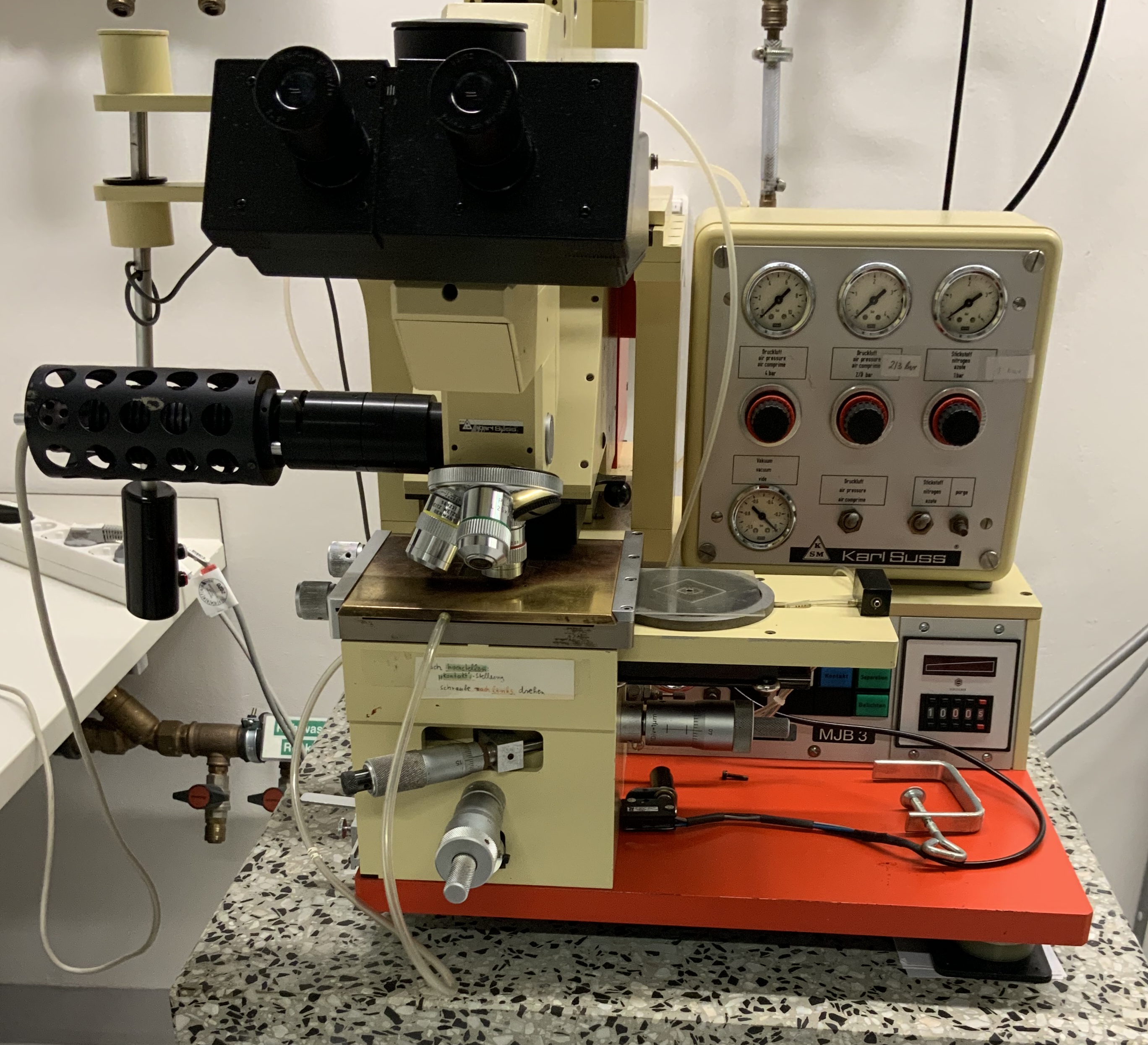
More on photolithography
|
|
Mask aligner (Süss MJB3, ancient... 😨).
Photo
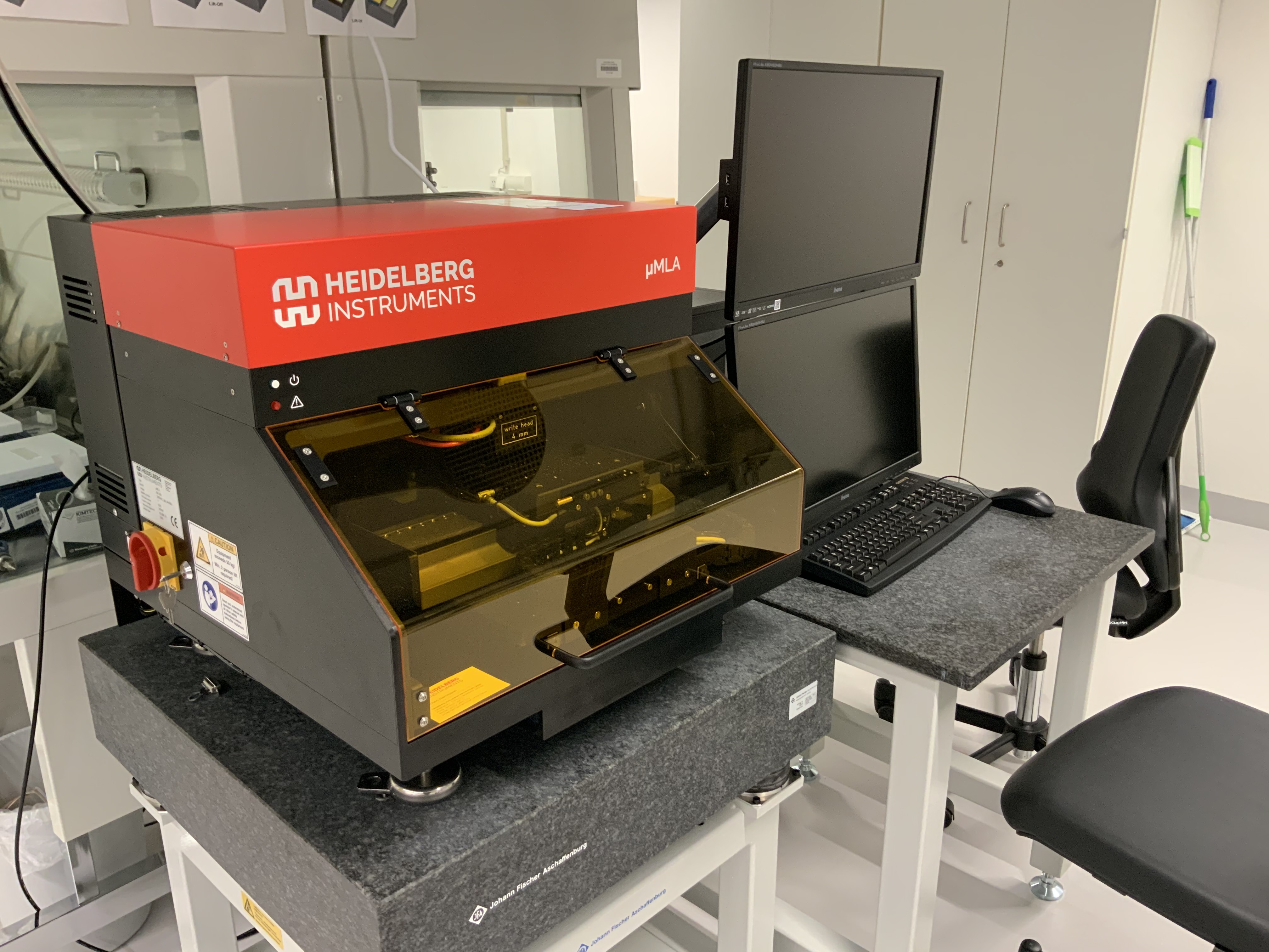
Direct write photolithography (μMLA, Heidelberg Instruments).
Photo
|
More on reactive ion etching
|
|
|
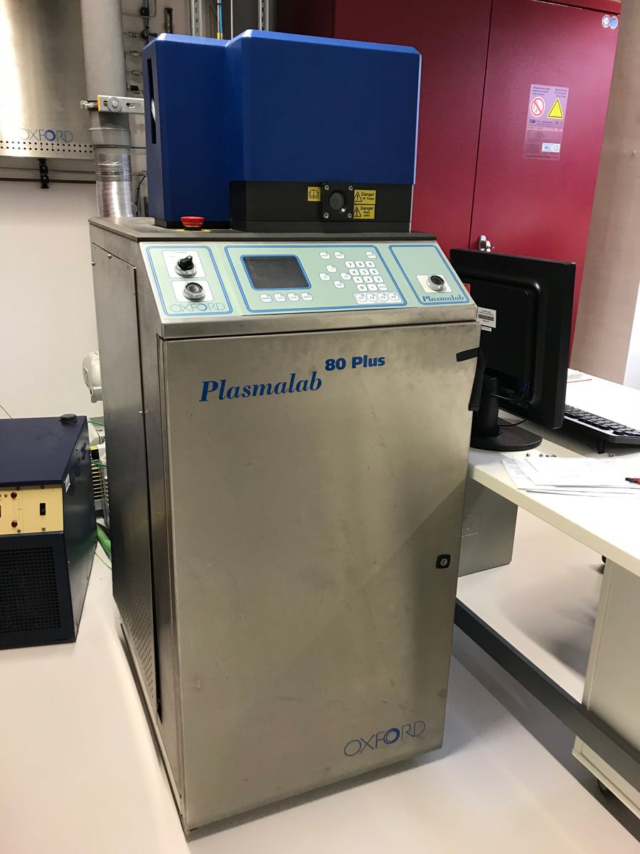
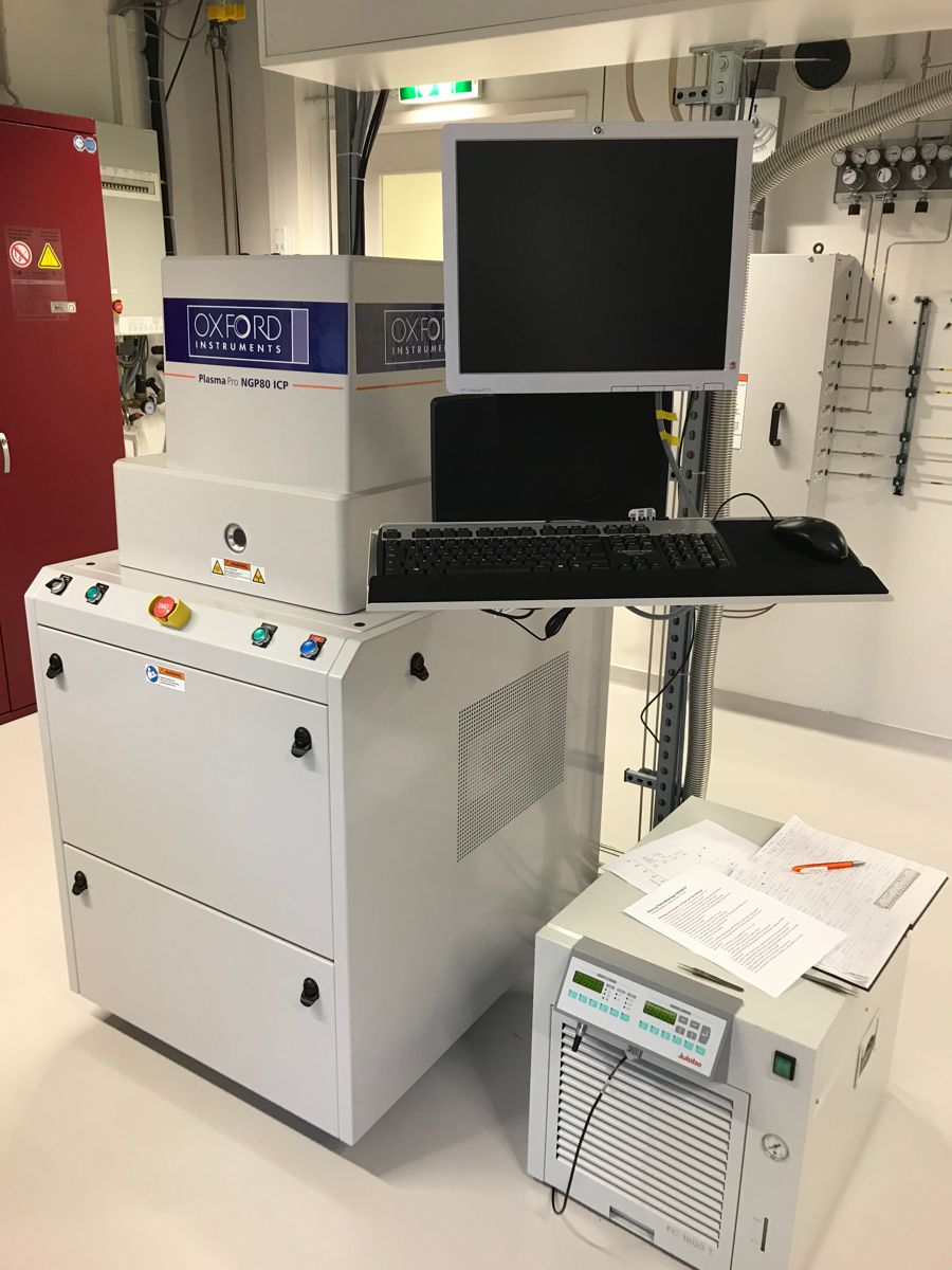
Reactive ion etching (PlasmaPro NGP80 ICP, Oxford) with inductively coupled plasma and fluorine-based chemistry.
Photo
|
| | |
|
Theory
We develop theories for optical modes in nano- and microstructures, anisotropic optics,
pseudomorphic strain in heterostructures and X-ray scattering among others.
More on theory
|
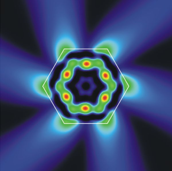
Modes in micro- and nano-sized optical resonators
Key publications
S. Richter, T. Michalsky, C. Sturm, B. Rosenow, M. Grundmann, R. Schmidt-Grund
Exceptional points in anisotropic planar microcavities
Phys. Rev. A 95, 023836 (2017) | doi
S. Richter, T. Michalsky, L. Fricke, C. Sturm, H. Franke, M. Grundmann, R. Schmidt-Grund
Maxwell consideration of polaritonic quasi-particle Hamiltonians in multi-level systems
Appl. Phys. Lett. 107, 231104 (2015) | doi
T. Nobis, M. Grundmann
Low order whispering gallery modes in hexagonal nanocavities
Phys. Rev. A 72, 063806 (2005) | doi
Stress and Strain
Key publications
M. Grundmann
A Most General and Facile Recipe for the Calculation of Heteroepitaxial Strain
phys. stat. sol. b XXX, 2000323 (2018) | doi
M. Grundmann
Elastic Theory of Pseudomorphic Monoclinic and Rhombohedral Heterostructures
J. Appl. Phys. 124, 185302 (2018) | doi
M. Grundmann
Strain in Pseudomorphic Monoclinic Ga2O3-based Heterostructures
phys. stat. sol. (b) 254, 1700134 (2017) | doi
M. Grundmann, J. Zúñiga-Pérez
Pseudomorphic ZnO-based heterostructures: from polar through all semipolar to nonpolar orientations
phys. stat. sol. (b) 253, 351-360 (2016) | doi
M. Grundmann
Theory of Semiconductor Solid and Hollow Nano- and Microwires With Hexagonal Cross-Section Under Torsion
phys. stat. sol. (b) 252, 773-785 (2015) | doi
Miscellaneous
Key publications
C. Kranert, C. Sturm, R. Schmidt-Grund, M. Grundmann
Raman Tensor Formalism for Optically Anisotropic Crystals
Phys. Rev. Lett. 116, 127401 (2016) | doi
M. Grundmann, M. Scheibe, M. Lorenz, J. Bläsing, A. Krost
X-ray multiple diffraction of ZnO substrates and heteroepitaxial thin films
phys. stat. sol. (b) 251, 850-863 (2016) | doi
|
|
| Funding is provided through the FUGG/HbfG and EFRE schemes as well as several cooperative projects
and individual grants. Most of our research is within the
university's research profile area
"Complex Matter".
|
| Image credits: P. Schlupp, Ch. Yang, Zh. Zhang, J. Lenzner, S. Richter, M. Lorenz, C. Kranert, T. Nobis, M. Grundmann, all Universität Leipzig.
|
|